This project was made possible by PCBWay, who sponsored the fabrication of the redesigned GigaShield v0.2 level converter board. PCBWay offers PCB prototyping, assembly, CNC machining, and 3D printing services, from one-off prototypes to production runs. If you have a PCB design ready to go, check them out at pcbway.com.
In January, I spent $468 on Fiverr to have a professional design an Arduino Giga R1 shield with level shifters. It was a good design. Nine TXB0108PW bidirectional level translators, 72 channels of 3.3V-to-5V shifting, a clean two-layer board ready for fabrication. And then I started testing it with the RetroShield Z80, and the auto-sensing level shifters fell apart.
The TXB0108 is a clever chip. It detects signal direction automatically, so you don't need to tell it whether a pin is input or output. For most applications, that's a feature. For a Z80 bus interface, it's a fatal flaw. During bus cycles, the Z80 tri-states its address and data lines. The outputs go high-impedance. They're not driving high or low, they're floating. The TXB0108 can't determine drive direction from a floating signal. It guesses wrong, or it doesn't drive at all, and the Arduino on the other side sees garbage. The board was blind to half of what the Z80 was doing.
The fix was clear: replace the TXB0108s with SN74LVC8T245PW driven level shifters. The SN74LVC8T245 has an explicit DIR pin: you tell it which direction to translate, and it does exactly that, regardless of whether the signals are being actively driven. No guessing, no ambiguity, deterministic behavior during tri-state periods. The trade-off is that you need a direction control signal for each shifter IC, but that's a small price for reliability.
What wasn't clear was how to execute the redesign. I could go back to Fiverr for another $400-500. I could spend weeks learning KiCad properly. Or I could try something that had worked surprisingly well on a previous project: use AI and open-source command-line EDA tools to design the board from a terminal, without ever opening a graphical PCB editor.
This is part one of a two-part series. This piece covers the design and toolchain: how I used Claude Code, the gEDA ecosystem, pcb-rnd, and Freerouting to go from a failed design to production-ready Gerber files. Part two will cover the physical boards, assembly, and testing against the Z80.
The Toolchain Problem
The original Fiverr design was done in KiCad 9.0. My first instinct was to modify it directly: swap the TXB0108 footprints for SN74LVC8T245, update the pin mappings, add the DIR control header, and re-route. But there was a problem. My preferred command-line PCB tool, pcb-rnd, is version 3.1.4 on Ubuntu. KiCad 9.0 uses a file format version (20241229) that pcb-rnd's io_kicad plugin doesn't support. When I tried to open the KiCad PCB:
unexpected layout version number (perhaps too new)
Hard stop. No conversion path exists from KiCad 9.0 to pcb-rnd. The formats aren't just different versions. KiCad's S-expression format and pcb-rnd's text-based format are fundamentally different syntaxes.
I could have started KiCad and used its GUI. But I'd already proven to myself with the dual Z80 RetroShield project that text-based, AI-assisted PCB workflows are not only possible but sometimes preferable. The gEDA/pcb-rnd file format is human-readable. AI can parse it, reason about it, and generate it. A Python script can manipulate it. You can diff two boards and see exactly what changed. None of that is true for a graphical-only workflow.
So the plan became: extract everything useful from the KiCad source files, then rebuild the board from scratch in pcb-rnd's native format using Python. Sound insane? It kind of is. But it worked.
Extracting the DNA
Even though pcb-rnd couldn't read the KiCad files directly, the KiCad files contained all the design intelligence I needed. Component positions, net assignments, pin mappings, board dimensions. It was all there, just in a format I couldn't import.
KiCad's CLI tools (kicad-cli) could export what I needed:
# Component positions (X, Y, rotation for each part)
kicad-cli pcb export pos AlexJ_bz_ArduinoGigaShield.kicad_pcb -o giga_pos.csv

# Netlist connectivity
kicad-cli pcb export ipc2581 AlexJ_bz_ArduinoGigaShield.kicad_pcb -o giga_netlist.d356
The schematic file (AlexJ_bz_ArduinoGigaShield.kicad_sch) was an S-expression text file I could parse to extract the signal mappings: which Giga pin connects to which 5V header pin through which level shifter channel. This was the most critical piece: getting the net assignments wrong would mean the board physically connects but logically doesn't work.
This is where Claude Code earned its keep. I described the KiCad schematic structure and asked it to help me parse out the signal mappings. The KiCad schematic uses hierarchical sheets with positional net connections, which isn't the simplest format to work with manually, but straightforward for an AI that can read S-expressions and track net names across sheets. Within an hour, I had a complete mapping of all 72 signal channels across the 9 shifter ICs.
Generating the Board with Python
With positions and nets extracted, I wrote build_giga_shield.py, a single Python script that generates the entire pcb-rnd board from scratch. No GUI involved. Every component footprint, every pin, every net connection is defined programmatically.
The script is structured around four generator functions:
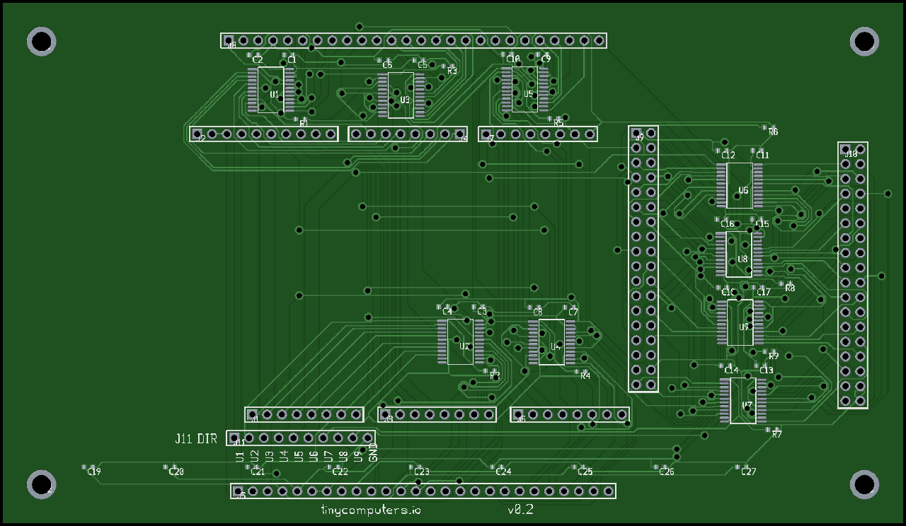
tssop24_element() generates the SN74LVC8T245PW footprint. TSSOP-24 is a precise geometry: 0.65mm pin pitch, 6.4mm pad-to-pad span, 24 pins. The function calculates pad positions mathematically: 12 pins on the left, 12 on the right, with pin 1 marked as square per convention. Getting the pin numbering right was critical. The SN74LVC8T245's datasheet shows pins 1-12 on the left (DIR, A1-A4, GND, A5-A8, OE#, GND) and pins 13-24 on the right counting bottom-to-top (B8-B5, VCCB, B4-B1, VCCA, VCCA, VCCB).
pin_header_element() handles through-hole pin headers with rotation support. The Arduino Giga R1 has an unusual form factor: the long pin headers run along the board edges horizontally, not vertically. In the original KiCad design, these were placed with 90-degree or -90-degree rotation. Without matching that rotation, a 26-pin header at y=84mm would extend 63.5mm downward to y=148mm, well past the 90mm board edge. The rotation transform was simple once identified:
def rotate(px, py):
    if rot == 90:
        return (py, -px)
    elif rot == -90:
        return (-py, px)
    return (px, py)
smd_0603_element() creates the 0603 footprint shared by all 27 decoupling capacitors and 9 pull-down resistors. Small SMD parts, simple geometry.
mounting_hole_element() places the four 3.2mm mounting holes that align with the Arduino Giga's standoff positions.
The coordinate system was the trickiest part. KiCad uses an arbitrary origin; in this design, x=106mm, y=30.5mm. pcb-rnd uses (0,0). Every KiCad coordinate had to be translated:
KX, KY = 106.0, 30.5
def kpos(kx, ky):
    return (mm(kx - KX), mm(ky - KY))
The build_pcb() function ties everything together: place components, assign nets, build the symbol table, generate the layer stack, and write out a valid pcb-rnd .pcb file. Running the script produces a complete, unrouted board: components placed, netlist defined, silkscreen text positioned, board outline drawn. Ready for routing.
$ python3 build_giga_shield.py
Generated giga_shield.pcb
Board: 155mm x 90mm
9x SN74LVC8T245PW (TSSOP-24) level shifters
DIR control via J11 (1x10 header)
The Format Wars
Getting pcb-rnd to actually accept the generated file was its own adventure. pcb-rnd's parser is strict about things that look optional in the documentation, and its error messages are sometimes misleading. An error in an Element definition might be reported as a syntax error in the Layer section fifty lines later.
Three format issues bit me hardest:
The "smd" flag. I initially generated elements with Element["smd" "TSSOP24" "U1" ...], which seemed logical for surface-mount parts. pcb-rnd rejected it with "Unknown flag: smd ignored," which cascaded into a complete parse failure. The fix: use an empty string Element["" "TSSOP24" "U1" ...]. The SMD-ness is implicit from using Pad[] entries instead of Pin[] entries.
Bare zeros. pcb-rnd is inconsistent about whether 0 and 0nm are interchangeable. In some contexts, bare 0 works fine. In others, it causes a silent parse error that manifests as a syntax error dozens of lines later. The defensive fix: always use 0nm, never bare 0, everywhere.
Missing flags on Layer lines. The Line[] entry inside Layer blocks needs 7 fields, not 6. The seventh is a flags string like "clearline". My generator omitted it, producing Line[x1 y1 x2 y2 thickness clearance]. The parser's error message: syntax error, unexpected ']', expecting INTEGER or STRING, reported at the layer definition, not at the malformed line.
I found these bugs using a binary search approach, truncating the file with head -N and testing each truncation point until I isolated which section introduced the failure. It's crude but effective when error reporting is unhelpful. Claude Code helped enormously here. I'd paste the error and the surrounding file content, and it would spot the structural issue faster than I could.
The pcb-rnd Ecosystem
For anyone unfamiliar with the tools involved, a brief orientation.
gEDA (GNU Electronic Design Automation) is a suite of open-source tools for electronic design. The original project dates to the late 1990s and includes gschem (schematic capture), pcb (PCB layout), and various utilities. The file formats are text-based and human-readable, a deliberate design choice that makes them scriptable and version-control-friendly. The original pcb program is now deprecated.
pcb-rnd is the actively maintained successor to gEDA's pcb program. It reads and writes the same text-based PCB format, but adds modern features: more export formats, better plugin support, and critically for this project, command-line export of Gerber files, PNG renderings, and Specctra DSN files. It runs on Linux (packaged for Ubuntu) but not macOS, which is why I ran it over SSH on a remote machine throughout this project.
Freerouting is a Java-based autorouter that speaks the Specctra DSN/SES interchange format. You feed it a board definition with components and nets but no traces, and it computes the copper routing, finding paths for every net while respecting design rules for trace width, clearance, and via placement. It's the open-source standard for PCB autorouting and has been used in production for decades.
The workflow chains these tools together:
build_giga_shield.py → giga_shield.pcb
                            ↓
                    [pcb-rnd DSN export]
                            ↓
                     giga_shield.dsn
                            ↓
                   [Freerouting autorouter]
                            ↓
                     giga_shield.ses
                            ↓
              [pcb-rnd SES import + Gerber export]
                            ↓
                    Production files
Every step is a command-line operation. Every intermediate file is text. Every transformation is reproducible. Change a component position in the Python script, re-run the pipeline, get new Gerber files. This is the power of text-based EDA: the entire design is version-controlled, diffable, and automatable.
Autorouting: The Machine Does the Tedious Part
With the board generated and validated in pcb-rnd, the next step was routing: connecting all 308 nets with actual copper traces across a two-layer board. This is where Freerouting comes in.
The pipeline starts with exporting the unrouted board to Specctra DSN format. pcb-rnd handles this in batch mode on the remote Linux machine:
pcb-rnd -x dsn giga_shield.pcb
The DSN file contains the board geometry, component placements, pad definitions, and netlist, everything the autorouter needs to compute a routing solution. One subtlety I learned the hard way: the DSN's (structure) section needs explicit (rule) and (via) definitions. pcb-rnd's DSN exporter puts the design rules inside the net class section, but Freerouting also expects them in the structure section. Without them, the router can see the nets but can't figure out what trace widths and via sizes are legal, and it silently fails to route most connections. A two-line addition fixed this:
(via pstk_1)
(rule
  (width 0.254)
  (clearance 0.254)
)
Freerouting itself is a Java application with both GUI and command-line modes. On my machine, I'm running a custom build from source. The current main branch had a few issues I had to fix (a missing static on the main method, a null pointer on maxThreads in the GUI initialization, and a Gradle build compatibility issue). The v1.9 codepath was more reliable for headless routing:
java -jar freerouting-1.9.0-executable.jar \
  -de giga_shield.dsn \
  -do giga_shield.ses
The autorouter loaded the 308-net board, ran through its passes, and produced a Specctra Session file containing 2911 wire segments and 172 vias. Every net connected. Every design rule satisfied. The routing took about 10 seconds for initial placement followed by optimization passes.
Importing the routes back into pcb-rnd was the final step. pcb-rnd can import SES files through its batch mode:
pcb-rnd --gui hid_batch giga_shield.pcb <<EOF
ImportSes(giga_shield.ses)
SaveTo(LayoutAs, giga_shield_routed.pcb)
EOF
The result: a fully routed PCB with 2911 traces and 172 vias, ready for Gerber export.
Running pcb-rnd Over SSH
One of the more unusual aspects of this project is that all pcb-rnd operations happened on a remote Ubuntu 24.04 machine accessed over SSH. pcb-rnd isn't available on macOS via Homebrew (I tried; there's a deprecated pcb package but no pcb-rnd), and building from source on macOS looked like a rabbit hole I didn't want to enter.
The remote workflow was straightforward:
# Upload the PCB
scp giga_shield.pcb alex@10.1.1.27:/tmp/

# Export DSN for routing
ssh alex@10.1.1.27 "pcb-rnd -x dsn /tmp/giga_shield.pcb"

# Import SES and export gerbers
ssh alex@10.1.1.27 'pcb-rnd --gui hid_batch /tmp/giga_shield.pcb <<EOF
ImportSes(/tmp/giga_shield.ses)
SaveTo(LayoutAs, /tmp/giga_shield_routed.pcb)
EOF'

# Export production files
ssh alex@10.1.1.27 "pcb-rnd -x gerber --gerberfile /tmp/giga_shield /tmp/giga_shield_routed.pcb"
ssh alex@10.1.1.27 "pcb-rnd -x png --dpi 600 --photo-mode --outfile /tmp/top.png /tmp/giga_shield_routed.pcb"

# Download results
scp alex@10.1.1.27:/tmp/giga_shield.*.gbr .
scp alex@10.1.1.27:/tmp/top.png giga_shield_top.png
It's more keystrokes than clicking Export in a GUI. But it's scriptable, repeatable, and fits into the same terminal where Claude Code is running. When I needed to iterate (move a component, re-route, re-export) I could do it in a single pipeline without switching contexts.
Claude Code as a Hardware Design Partner
I should be explicit about what Claude Code did and didn't do in this project, because the AI angle is the part people will either find most interesting or most suspicious.
What Claude Code did:
- Parsed the KiCad schematic to extract the 72-channel signal mapping across 9 level shifter ICs
- Wrote the initial
build_giga_shield.pygenerator script, including all four footprint generators and the net assignment logic - Debugged pcb-rnd format issues by analyzing error messages and file structure
- Managed the remote SSH workflow: uploading files, running pcb-rnd commands, downloading results
- Fixed bugs in the Freerouting build (the
static mainissue, the nullmaxThreads, the GradlefileModeAPI change) - Handled iterative changes: "move tinycomputers.io down by a millimeter" became an edit to the Python script, a regeneration, a re-import, and a re-export, all executed as a single flow
What Claude Code didn't do:
- Make architectural decisions. The choice to use SN74LVC8T245 over TXB0108, the DIR control header design, the decision to use pull-down resistors defaulting to A-to-B direction. Those were my decisions based on understanding the Z80 bus protocol; it is also on me for selecting the TXB0108 in the first place
- Verify electrical correctness. I checked the SN74LVC8T245 datasheet pin mapping myself. I verified that OE# tied to GND means always-enabled. I confirmed the 10K pull-down value was appropriate for the DIR pin
- Replace domain knowledge. I knew why the TXB0108 failed during tri-state periods because I understand Z80 bus cycles. Claude Code could have looked up the TXB0108 datasheet, but it couldn't have diagnosed the real-world failure mode from first principles
The pattern that emerged was: I made design decisions, Claude Code implemented them. I said "the DIR pins need pull-down resistors to default A-to-B direction," Claude Code generated the pcb-rnd Element entries with the correct footprint, position, and net assignments. I said "export gerbers at 600 DPI with photo mode," Claude Code ran the right pcb-rnd command on the remote machine.
This is the same division of labor I described in the dual Z80 post: I bring the domain knowledge, the AI handles the format translation. The text-based nature of gEDA files makes this work. If the design lived in a binary format or required mouse interactions, the AI would have been far less useful.
The New Design
Here's what the redesigned board looks like:
| Parameter | v0.1 (Fiverr/TXB0108) | v0.2 (Claude Code/SN74LVC8T245) |
|---|---|---|
| Level Shifter IC | TXB0108PW (TSSOP-20) | SN74LVC8T245PW (TSSOP-24) |
| Direction Control | Auto-sensing | Explicit DIR pin |
| Channels | 72 | 72 |
| Shifter ICs | 9 | 9 |
| Decoupling Caps | 27 | 27 |
| Pull-down Resistors | 9 (OE) | 9 (DIR) |
| DIR Control Header | None | J11 (1x10) |
| Board Dimensions | 155mm x 90mm | 155mm x 90mm |
| Layers | 2 | 2 |
| Design Tool | KiCad 9.0 (GUI) | Python + pcb-rnd (CLI) |
| Design Cost | $468.63 | $0 (open source tools) |
| Design Time | ~10 days (outsourced) | ~2 days (with AI) |
The J11 header is the key addition. It's a 1x10 pin header with 9 direction control pins (one per shifter IC) and a ground reference. Each DIR pin has a 10K pull-down resistor that defaults the direction to A-to-B (3.3V to 5V). To reverse a shifter's direction (for example, when the Arduino needs to read from the Z80's data bus) you drive the corresponding J11 pin high. The Arduino firmware manages this dynamically during bus cycles.
The board carries "tinycomputers.io" and "v0.2" on the silkscreen, placed near the bottom edge. Version tracking on the physical board, a lesson learned from the Fiverr experience, where I had to pay $57 for a revision just to add version text to the silkscreen.
Generating Production Files
With the routed board in hand, the final step was generating files suitable for manufacturing. pcb-rnd handles this with command-line exporters:
# Gerber files (9 layers: top/bottom copper, mask, silk, paste, outline, drill, fab)
pcb-rnd -x gerber --gerberfile giga_shield giga_shield_routed.pcb

# Photo-realistic renderings
pcb-rnd -x png --dpi 600 --photo-mode --outfile top.png giga_shield_routed.pcb
pcb-rnd -x png --dpi 600 --photo-mode --photo-flip-x --outfile bottom.png giga_shield_routed.pcb
The Gerber output includes everything a fab house needs: top and bottom copper, solder mask, silkscreen, paste stencil, board outline, and drill locations. The photo-realistic PNG renderings use pcb-rnd's built-in renderer: green solder mask, gold-plated pads, white silkscreen text. They're useful for documentation and for sanity-checking the layout before sending it to fabrication.
The BOM and centroid files were generated separately from the Python script's component data. The centroid file lists every SMD component's X/Y position and rotation, which is essential if you're having the boards assembled by a service rather than hand-soldering.
What's Different About This Approach
The standard way to design a PCB in 2026 is: open KiCad or Altium, draw a schematic, assign footprints, lay out the board, route traces (manually or with the built-in autorouter), and export Gerbers. It's a visual, interactive process that works well for most people and most projects.
What I did is different in a few ways that I think are worth noting, even if they're not universally applicable:
The entire design is a Python script. build_giga_shield.py is the single source of truth. Want to move a component? Change a coordinate in the script. Want to add a net? Add it to the dictionary. Want to change every decoupling cap from 0.1uF to 0.22uF? Change a string. Then re-run the pipeline. There's no "did I save the layout?" ambiguity, no undo history to worry about, no risk of accidentally moving something with a stray mouse click.
Every intermediate file is text. The .pcb file, the .dsn file, the .ses file. All text, all diffable, all version-controllable. When I moved a component and re-routed, I could git diff the PCB file and see exactly what changed. Try that with a binary PCB format.
AI can participate meaningfully. Because the files are text, Claude Code could read them, modify them, and verify them. It could grep for a component reference in the PCB file, find its coordinates, suggest a new position, and make the edit. It could read the Freerouting log and diagnose why routing failed. This level of AI participation simply isn't possible with graphical-only workflows.
The workflow is reproducible. I can hand someone the Python script and the Freerouting JAR and they can regenerate the entire board from scratch, on any machine with Python and Java. No KiCad version compatibility issues, no plugin dependencies, no "works on my machine" problems.
The trade-off is obvious: this approach requires understanding file formats at a level that graphical tools abstract away. If pcb-rnd's parser rejects your file with a misleading error message, you need to debug the file format, not just re-click a button. It's a power-user workflow. But for someone comfortable with text editors and command lines (which describes most of the audience reading a blog called tinycomputers.io), it's a viable alternative.
What's Next
The Gerber files are ready for fabrication. In part two, I'll cover ordering the boards from PCBWay, sourcing the SN74LVC8T245PW and passive components, and the moment of truth: plugging the RetroShield Z80 into the new shield and seeing if the Arduino can finally see the Z80's bus cycles clearly.
I'll also compare the v0.2 board side-by-side with the original Fiverr v0.1 board: the TXB0108 auto-sensing design versus the SN74LVC8T245 driven design. Same board dimensions, same connector layout, fundamentally different level-shifting approach. The comparison should be instructive for anyone choosing between auto-sensing and driven level translators for bus interfaces.
The Python build script, pcb-rnd source files, Gerber outputs, and all helper scripts are open source:
- giga-shield: Complete design files, build pipeline, and production outputs
This is part one of a two-part series. Part two will cover fabrication, assembly, and testing.
Previous posts in this series: Fiverr PCB Design ($468) · Dual Z80 RetroShield · CP/M on the Giga R1 · Zork on the Giga