This is the third post in a series about running CP/M 2.2 on a real Z80 processor connected to an Arduino Giga R1 WiFi. The first post covered getting the custom level converter shield designed and manufactured. The second post documented the hardware stack, the catastrophic TXB0108 level converter failures, the shadow register workaround, and the Rust sector server that provides disk I/O over WiFi. That post ended with a promise: CP/M was close to booting, and all the pieces were in place.
This post is about keeping that promise. It covers the final debugging push from "almost boots" to a fully interactive game of Zork I running on real Z80 hardware, and the performance crisis that nearly made the whole thing unusable.
The Story So Far
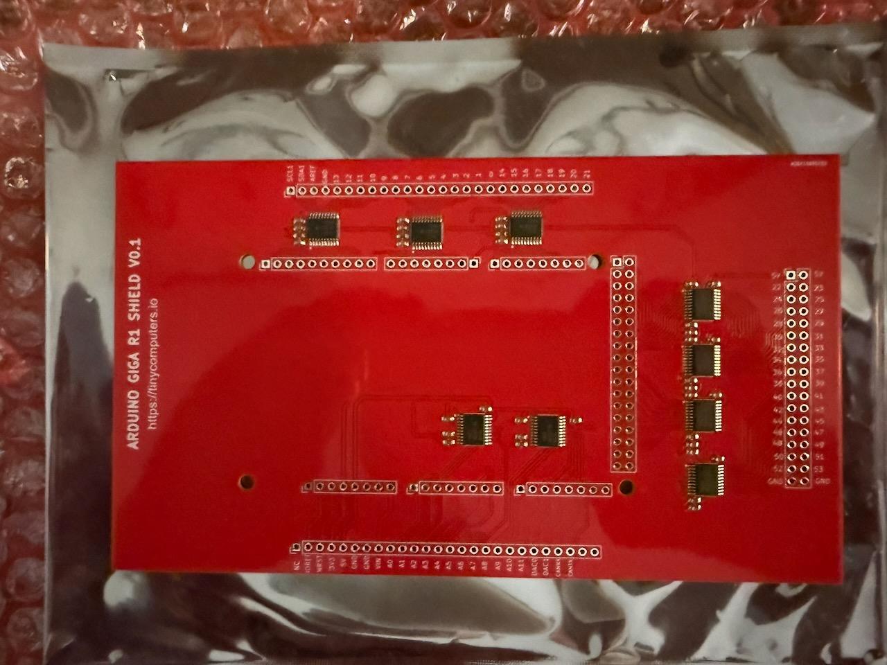
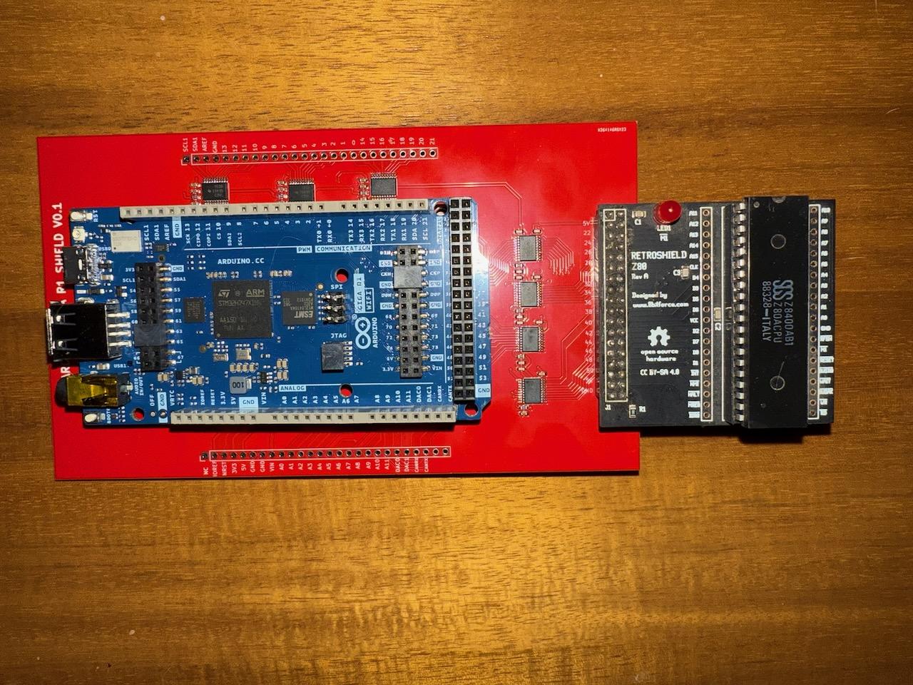
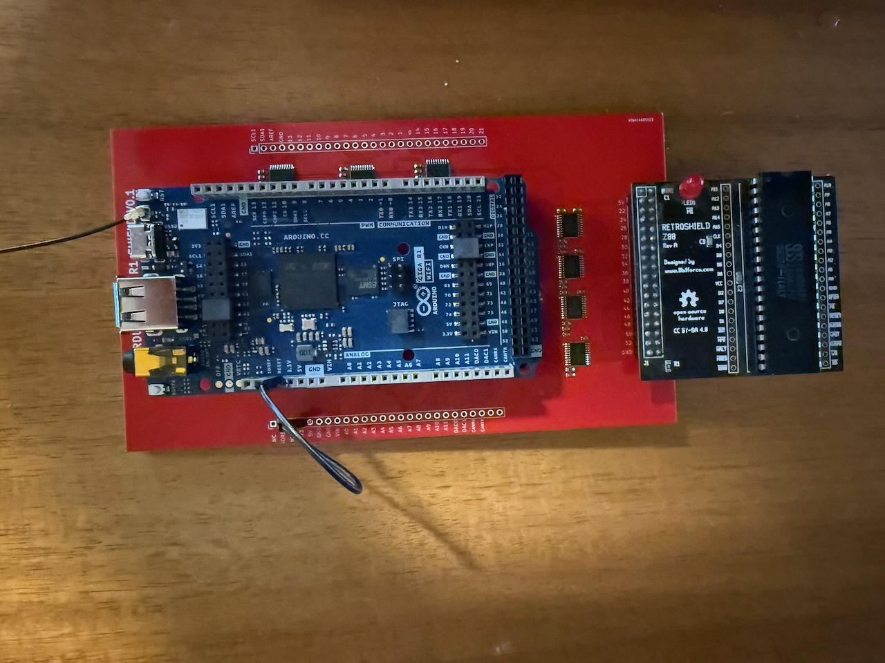
The hardware is straightforward: a RetroShield Z80 (a real Zilog Z80 CPU on a shield board) plugged into an Arduino Giga R1 WiFi through a custom level converter PCB. The Giga's STM32H747 (480MHz Cortex-M7) provides 64KB of Z80 RAM as a byte array in its internal SRAM, clocks the Z80, and serves memory read/write requests. Disk I/O goes over WiFi to a Rust TCP sector server instead of an SD card.
The level converter uses nine TXB0108 bidirectional level shifters to bridge the Giga's 3.3V logic and the RetroShield's 5V. And those TXB0108s are the source of almost every interesting engineering decision in the project. Their auto-direction sensing fails for several Z80 bus signals: IORQ_N and RD_N are permanently stuck, WR_N only works during memory cycles, and the data bus is invisible from Z80-to-Arduino during I/O operations. The address bus works but lags by 1-3 clock ticks through the converter.
These failures forced a fundamentally different approach to interfacing with the Z80. Instead of passively watching bus signals, the Arduino actively decodes the Z80's instruction stream and maintains software copies of the CPU's internal state:
-
Guard-only M1 detection: a timing table (
tStates[256]) tells us how many clock cycles each instruction takes; the next memory read after the guard expires is the next opcode fetch - Software PC (softPC): a software copy of the Z80's program counter, immune to address bus lag
-
Shadow registers: software copies of A, B, C, D, E, H, L, F, and SP, updated by decoding each opcode from
z80RAM[softPC] -
Pre-writes: memory store instructions write their values directly to
z80RAMat opcode detection time, using shadow register values and softPC-derived addresses, because the Z80's physical bus writes go to wrong addresses due to the propagation delay -
Deferred writes: for read-modify-write instructions like
INC (HL), where pre-writing would cause the Z80 to read an already-modified value and double-apply the operation
The full technical details of this architecture are in the previous post. What matters here is where that post left off: the shadow register system was working, the sector server was serving disk images over WiFi, and partial serial output confirmed that the Z80 was executing real code. What remained was completeness testing, making sure every instruction the Z80 actually executed was tracked correctly in the shadows.
CP/M Boots
The first milestone came faster than expected. After expanding the shadow register switch statement to cover more of the Z80 instruction set (POP instructions, ADD HL with register pairs, DAA (decimal adjust), EX (SP),HL), CP/M booted.
The boot loader loaded all 53 sectors of CPM.SYS from the sector server over WiFi. The BIOS cold boot initialized correctly. And the console printed:
RetroShield CP/M 2.2
56K TPA

a>
A real Z80, running real CP/M 2.2, with 56KB of Transient Program Area, booting from a disk image served over WiFi from a Rust TCP server. The DIR command worked and showed the contents of drive A:
a>dir
A: ZORK1    COM : ZORK1    DAT : ZORK2    COM : ZORK2    DAT
Zork was right there, waiting.
The "Bad Load" Bug
Running ZORK1.COM produced a single line of output and then nothing:
a>zork1
Bad load
"Bad load" is a CP/M CCP (Console Command Processor) error. It means the CCP tried to load the .COM file into the TPA and something went wrong: either a disk read failed, or the CCP's internal logic decided the load was corrupt.
Finding the Root Cause
The CCP loads .COM files by repeatedly calling BDOS function 20 (Read Sequential), advancing the DMA address by 128 bytes after each successful sector read, until the file is fully loaded. The load loop lives in the CCP code at address 0xE6DE. After each BDOS call, it checks whether the DMA address has exceeded the TPA boundary at 0xE000:
E6F5: LD E,A         ; save BDOS return code
E6F6: LD A,H         ; get current DMA high byte
E6F7: SUB E           ; compare against...
E6F8: LD A,H          ; (for SBC below)
E6F9: SBC A,D         ; ...TPA boundary
E6FB: JP NC,E771      ; if past TPA, stop loading
The SBC A,D instruction at E6F9 (opcode 0x9A) subtracts the D register and the carry flag from A. This is a 16-bit comparison implemented as a high-byte subtract-with-borrow after the low-byte subtract at E6F7.
The problem: opcode 0x9A was not in the shadow register tracking. The switch statement had SBC A,A (0x9F), SBC A,B (0x98), and SBC A,C (0x99), but not SBC A,D.
Without tracking, the SBC A,D instruction didn't update shadowF. The carry flag in the shadow still reflected the preceding SUB E instruction, which had set carry=0 (no borrow, since 0x80 - 0x00 = 0x80). But the real Z80 computed SBC A,D with the actual register values and got carry=1 (borrow). When the JP NC,E771 branch came, our shadow said NC=true (carry clear, branch taken) while the Z80 said NC=false (carry set, branch not taken).
SoftPC jumped to the "Bad load" error handler. The real Z80 continued the load loop. From that point on, softPC and the Z80's actual program counter were desynchronized; every subsequent opcode decode was wrong, and the system was effectively running blind.
The Fix
Add the missing instructions. All of them:
// SBC A,r — subtract with carry
case 0x98: { uint16_t r = shadowA - shadowB - (shadowF & FLAG_C ? 1 : 0);
             shadowF = flagsSub8(shadowA, shadowB, r, true);
             shadowA = r & 0xFF; break; }
case 0x99: { /* SBC A,C */ ... }
case 0x9A: { /* SBC A,D */ ... }
case 0x9B: { /* SBC A,E */ ... }
case 0x9C: { /* SBC A,H */ ... }
case 0x9D: { /* SBC A,L */ ... }
case 0x9E: { /* SBC A,(HL) */ ... }

// ADC A,r — add with carry (same gap)
case 0x8A: { /* ADC A,D */ ... }
case 0x8B: { /* ADC A,E */ ... }
case 0x8C: { /* ADC A,H */ ... }
case 0x8D: { /* ADC A,L */ ... }
case 0x8E: { /* ADC A,(HL) */ ... }
After this fix, ZORK1.COM loaded all 68 sectors successfully: 8,704 bytes from DMA address 0x0100 to 0x2300, with every BDOS read returning success.
Zork Starts, Barely
With the load fixed, Zork launched. It read its .DAT file from disk. The copyright text appeared:
ZORK I: The Great Underground Empire
Copyright (c) 1981, 1982, 1983 Infocom, Inc. All rights
reserved.
ZORK is a registered trademark of Infocom, Inc.
Revision 88 / Serial number 840726
And then... nothing. Or rather, something, but at glacial speed. At approximately 18,000 Z80 clock cycles per second, the text took minutes to render. The game was technically running but practically frozen. Typing a command and waiting for a response meant staring at a blank terminal for an eternity.
On a 480MHz Cortex-M7, 18,000 Z80 cycles per second means the Arduino was spending roughly 26,000 of its own CPU cycles on every single Z80 clock tick. Something was catastrophically wrong with the hot loop.
The Performance Crisis
I added a performance counter that measured actual Z80 cycles per second. The numbers were dire: 9,000–18,000 cycles/sec depending on what the Z80 was doing. A real Z80 runs at 2.5–8 MHz. We were three orders of magnitude too slow.
Five bottlenecks were hiding in the hot loop, each one multiplying the others.
Bottleneck 1: A Two-Millisecond Nap on Every Tick
Every clock tick included delayMicroseconds(2), a 2,000-nanosecond delay to let signals settle through the TXB0108 after toggling the clock. The TXB0108's actual propagation delay is about 4–12 nanoseconds. This was a 200x safety margin I'd added early in debugging and never removed.
Fix: Replace with 24 inline NOP instructions. At 480MHz, each NOP is ~2ns, giving roughly 50ns of settle time, still 4x more than the TXB0108 needs, but 40x faster than the delay.
inline void __attribute__((always_inline)) busSettle() {
    __asm volatile("nop\nnop\nnop\nnop\nnop\nnop\nnop\nnop\n"
                   "nop\nnop\nnop\nnop\nnop\nnop\nnop\nnop\n"
                   "nop\nnop\nnop\nnop\nnop\nnop\nnop\nnop\n");
}
Bottleneck 2: Flipping 8 Pins on Every Single Tick
This was the real killer. At the end of every cpu_tick() call, setDataBusInput() was called to tri-state the data bus pins, switching all 8 data lines from output to input mode. Then at the start of the next memory read, setDataBusOutput() switched them all back. Each direction change went through the Arduino HAL pinMode() function 8 times.
On the STM32H747 with the mbed-based Arduino core, each pinMode() call involves HAL abstraction layers, pin table lookups, and clock configuration checks. Eight calls took approximately 16–32 microseconds. This was happening on every single clock tick, both directions, 16 pinMode() calls per tick.
The irony: this direction switching was completely unnecessary. Since all Z80 bus writes are suppressed (pre-writes handle memory stores in software), the data bus never needs to read anything from the Z80 during normal operation. The bus can stay in output mode permanently.
Fix: Remove the per-tick setDataBusInput() call entirely. For the rare cases where direction changes are still needed (certain IO operations), replace pinMode() with direct GPIO MODER register writes:
#define GPIO_SET_OUTPUT(port, pin) \
    ((port)->MODER = ((port)->MODER & ~(3U << ((pin)*2))) \
                     | (1U << ((pin)*2)))
#define GPIO_SET_INPUT(port, pin) \
    ((port)->MODER = ((port)->MODER & ~(3U << ((pin)*2))))
One register write per pin instead of a full HAL function call.
Bottleneck 3: Arduino HAL in the Hot Loop
The Arduino digitalRead() and digitalWrite() functions are convenient abstractions, but on the STM32H747 they carry significant overhead: pin number lookups, port mapping tables, multiple function calls per operation. The original RetroShield code for the Mega 2560 used direct AVR port registers (PORTA, PORTL) for fast parallel I/O. On the Giga, the pins are scattered across GPIO ports B, E, G, H, I, J, and K (no single-register solution), but direct register access is still orders of magnitude faster than the HAL.
Fix: Map every Arduino pin to its STM32H747 GPIO port and pin number, then replace all hot-path I/O with direct register access.
The clock signal (toggled every tick) went from ~200ns per call through HAL to ~4ns via the BSRR (Bit Set/Reset Register):
// Before
#define CLK_HIGH  digitalWrite(uP_CLK, HIGH)

// After — single atomic register write
#define CLK_HIGH  (GPIOK->BSRR = (1U << 2))    // PK2
#define CLK_LOW   (GPIOK->BSRR = (1U << 18))   // PK2 reset
The BSRR register is an elegant STM32 feature: bits [15:0] set outputs high, bits [31:16] set outputs low, and the entire operation is atomic, so no read-modify-write cycle is needed.
For the address bus (16 pins read every memory cycle), three GPIO IDR (Input Data Register) reads replace sixteen individual digitalRead() calls:
inline uint16_t readAddress() {
    uint32_t jIDR = GPIOJ->IDR;
    uint32_t kIDR = GPIOK->IDR;
    uint32_t gIDR = GPIOG->IDR;

    uint16_t addr = 0;
    if (jIDR & (1U << 12)) addr |= (1 << 0);   // A0 = PJ12
    if (gIDR & (1U << 13)) addr |= (1 << 1);   // A1 = PG13
    // ... 14 more bit extractions
    return addr;
}
For the data bus (8 pins written every memory read cycle), pins sharing the same GPIO port are combined into a single BSRR write. Port I has three data bus pins, so they get folded into one register operation:
inline void writeDataBus(byte val) {
    GPIOE->BSRR = (val & 0x01) ? (1U << 4) : (1U << 20);
    GPIOK->BSRR = (val & 0x02) ? (1U << 0) : (1U << 16);
    GPIOB->BSRR = (val & 0x04) ? (1U << 2) : (1U << 18);
    GPIOH->BSRR = (val & 0x08) ? (1U << 15) : (1U << 31);

    // Port I: combine 3 data bus pins into one write
    uint32_t iBSRR = 0;
    iBSRR |= (val & 0x10) ? (1U << 13) : (1U << 29);  // PI13
    iBSRR |= (val & 0x40) ? (1U << 10) : (1U << 26);  // PI10
    iBSRR |= (val & 0x80) ? (1U << 15) : (1U << 31);  // PI15
    GPIOI->BSRR = iBSRR;

    GPIOG->BSRR = (val & 0x20) ? (1U << 10) : (1U << 26);
}
Bottleneck 4: USB Serial Polling Every Tick
The MC6850 ACIA emulation checked Serial.available() on every clock tick to detect incoming keystrokes. On the Giga, USB CDC serial operations are expensive; each call may involve USB stack processing. At 700K ticks/sec, checking every tick means 700,000 USB stack queries per second.
Fix: Check every 256 ticks. That's still a 2,700 Hz polling rate, more than fast enough for interactive typing, and it eliminates 99.6% of the USB overhead.
if ((clock_cycle_count & 0xFF) == 0) {
    if (!CONTROL_RTS_STATE && Serial.available()) {
        reg6850_STATUS |= 0b00000001;   // RDRF set
        if (CONTROL_RX_INT_ENABLE) { INT_N_LOW; }
    }
}
Bottleneck 5: I-Cache Thrashing from Forced Inlining
The cpu_tick() function is around 1,200 lines of code, dominated by the shadow register tracking switch statement with hundreds of cases. It was marked inline __attribute__((always_inline)), which forces the compiler to inline the entire function body into loop().
The STM32H747's instruction cache is 16KB. Inlining a 1,200-line function creates a binary blob that doesn't fit, causing constant cache misses. Every iteration of the main loop refills the I-cache from flash.
Fix: Change to __attribute__((noinline)). The function call overhead (a few nanoseconds for the branch and return) is negligible compared to the cache thrashing cost. This change also reduced the compiled binary by ~9KB, from 284KB to 276KB.
void __attribute__((noinline)) cpu_tick() {
    // ... 1,200 lines of bus interface and shadow tracking
}
The Result
| Metric | Before | After |
|---|---|---|
| Z80 cycles/sec | ~9,000 | ~690,000 |
| Effective Z80 clock | ~0.009 MHz | ~0.69 MHz |
| Binary size | 284 KB | 276 KB |
| Time per Z80 tick | ~111 µs | ~1.4 µs |
A 75x speedup. The system went from roughly 50,000 Cortex-M7 cycles per Z80 tick down to about 700. Enough for Zork to be fully interactive.
Network Reconnection
With the performance problem solved, a new issue appeared: the TCP connection to the sector server dropped during long idle periods. Zork is a text adventure; the player types a command, the game responds, and then nothing happens until the next command. During that idle time (which could be minutes while you think about whether to go north or east), the WiFi TCP socket would quietly die. The next disk operation would fail with "Bad Sector."
The fix was automatic reconnection logic. Before each disk operation, ensureServerConnection() checks if the TCP socket is still alive. If not, it reconnects to the sector server, re-opens the disk image file that was previously open, and re-seeks to the last position, all transparently, so the Z80 never knows the connection dropped.
bool ensureServerConnection() {
    if (server.connected()) return true;

    Serial.println("[NET] Connection lost, reconnecting...");
    server.stop();

    for (int attempt = 0; attempt < 3; attempt++) {
        if (server.connect(SERVER_IP, SERVER_PORT)) {
            Serial.println("[NET] Reconnected to server");
            if (diskFileOpen && diskActiveFile.length() > 0) {
                netSendFileCommand(DISK_CMD_OPEN_RW, diskActiveFile);
                uint8_t status = netReadStatus();
                if (status != 0) { diskFileOpen = false; return false; }
                // Re-seek to last known position
                uint8_t seekCmd[4];
                seekCmd[0] = DISK_CMD_SEEK;
                seekCmd[1] = diskSeekPos & 0xFF;
                seekCmd[2] = (diskSeekPos >> 8) & 0xFF;
                seekCmd[3] = (diskSeekPos >> 16) & 0xFF;
                server.write(seekCmd, 4);
                netReadStatus();
            }
            return true;
        }
        delay(500);
    }
    return false;
}
Playing Zork
With all the pieces in place (shadow registers covering every instruction CP/M and Zork use, GPIO registers replacing Arduino HAL calls, network reconnection handling idle timeouts), it was time to play.
Here's a complete boot-to-gameplay session, captured from the serial terminal:
OK (192.168.0.75)
Server:     OK (192.168.0.248:9000)
Boot:       OK (512 bytes loaded)

Starting Z80...

RetroShield Z80 Boot Loader
Copyright (c) 2025 Alex Jokela, tinycomputers.io

Loading CPM.SYS.....................................................
Boot complete.

RetroShield CP/M 2.2
56K TPA

a>zork1
ZORK I: The Great Underground Empire
Copyright (c) 1981, 1982, 1983 Infocom, Inc. All rights
reserved.
ZORK is a registered trademark of Infocom, Inc.
Revision 88 / Serial number 840726

West of House
You are standing in an open field west of a white house, with
a boarded front door.
There is a small mailbox here.

>open mailbox
Opening the small mailbox reveals a leaflet.

>take leaflet
Taken.

>go south
South of House
You are facing the south side of a white house. There is no
door here, and all the windows are boarded.

>go east
Behind House
You are behind the white house. A path leads into the forest
to the east. In one corner of the house there is a small
window which is slightly ajar.

>open window
With great effort, you open the window far enough to allow
entry.

>enter
Kitchen
You are in the kitchen of the white house. A table seems to
have been used recently for the preparation of food. A passage
leads to the west and a dark staircase can be seen leading
upward. A dark chimney leads down and to the east is a small
window which is open.
On the table is an elongated brown sack, smelling of hot
peppers.
A bottle is sitting on the table.
The glass bottle contains:
  A quantity of water
Every command produces the correct response, at interactive speed. The text appears as fast as you'd expect from a terminal session, with no perceptible delay between pressing Enter and seeing the game's response.
How It All Fits Together
Here's what happens when you type open mailbox at the Zork prompt, end to end:
-
Each keystroke arrives over USB serial. Every 256 Z80 clock ticks, the Arduino checks
Serial.available(), finds a character, and sets the MC6850 ACIA status register's RDRF bit. -
The Z80 is spinning in the BIOS console input loop, repeatedly executing
IN A,(0x80)to check the ACIA status register. Our shadow register system detects eachINinstruction at M1 time, callshandle_io_read(0x80), and drives the status byte onto the data bus during the IO cycle. -
When RDRF is set, the Z80 executes
IN A,(0x81)to read the character. We return the byte fromSerial.read(), andshadowAgets updated to match. -
The BIOS echoes the character by executing
OUT (0x81),A. We detect this at M1 time, useshadowAfor the data value, and callSerial.write(). -
When the user presses Enter, the CCP passes the command to Zork. Zork parses it and starts executing game logic, hundreds of thousands of Z80 instructions manipulating its internal data structures.
-
When Zork needs to read from its
.DATfile, the BIOS executes a sequence ofOUTinstructions to set up the disk operation: filename characters to port0x13, seek position to ports0x14/0x15/0x19, DMA address to ports0x16/0x17, and a block read command to port0x18. EachOUTis intercepted by the shadow register system and forwarded to the sector server over WiFi. -
The sector server reads 128 bytes from the disk image file, sends them back over TCP. The Arduino writes them directly into
z80RAMat the DMA address. -
Zork processes the data, generates response text, and prints it character by character through the ACIA, each character going through the same
OUT (0x81),A→shadowA→Serial.write()path.
Every single one of these operations relies on the shadow register system. The Z80 has no idea the Arduino can't see half its bus signals. It thinks it's talking to normal memory and I/O ports. The Arduino, meanwhile, is running a parallel simulation of the Z80's register state, intercepting every instruction, and making the illusion seamless.
The Full Architecture
For reference, here's the complete technical stack:
Hardware: - Arduino Giga R1 WiFi (STM32H747, 480MHz Cortex-M7, 1MB SRAM, WiFi) - RetroShield Z80 (real Zilog Z80 CPU, 5V logic) - Custom level converter PCB (nine TXB0108PW, design details here)
Z80 Memory:
- 64KB byte array in Giga's internal SRAM (uint8_t z80RAM[65536])
Bus Interface (direct STM32 GPIO registers): - Clock: GPIOK pin 2 (BSRR for set/clear) - Address: 3 IDR reads (GPIOJ, GPIOK, GPIOG) → 16-bit extraction - Data: 6 BSRR writes (GPIOE, GPIOK, GPIOB, GPIOH, GPIOI combined, GPIOG) - Control: MREQ via GPIOK pin 7, WR via GPIOE pin 6
Software Architecture:
- Guard-only M1 detection with tStates[256] timing table
- Software PC tracking (softPC) for all branch types including conditional
- Shadow registers (A, B, C, D, E, H, L, F, SP) with full ALU flag computation
- Pre-writes for all memory store instructions
- Deferred writes for read-modify-write instructions (INC/DEC (HL), CB prefix on (HL))
- IO handling at M1 time using shadow register values
Disk I/O: - Rust TCP sector server on local network (192.168.0.248:9000) - 128-byte CP/M sector transfers over WiFi - Automatic reconnection with file re-open and seek restore
Console I/O: - Emulated MC6850 ACIA on ports 0x80/0x81 - USB CDC serial at 115200 baud - Interrupt-driven receive with throttled polling (every 256 ticks)
Pin Mapping Reference
For anyone attempting a similar project, here's the complete mapping from Arduino digital pins to STM32H747 GPIO ports. This is essential for the direct register access that makes the performance optimization possible:
| Function | Arduino Pin | STM32 Port/Pin |
|---|---|---|
| CLK | D52 | PK2 |
| MREQ_N | D41 | PK7 |
| WR_N | D40 | PE6 |
| IORQ_N | D39 | PI14 |
| INT_N | D50 | PI11 |
| RESET_N | D38 | PJ7 |
| Data bit 0 | D49 | PE4 |
| Data bit 1 | D48 | PK0 |
| Data bit 2 | D47 | PB2 |
| Data bit 3 | D46 | PH15 |
| Data bit 4 | D45 | PI13 |
| Data bit 5 | D44 | PG10 |
| Data bit 6 | D43 | PI10 |
| Data bit 7 | D42 | PI15 |
| Addr A0 | D22 | PJ12 |
| Addr A1 | D23 | PG13 |
| Addr A2 | D24 | PG12 |
| Addr A3 | D25 | PJ0 |
| Addr A4 | D26 | PJ14 |
| Addr A5 | D27 | PJ1 |
| Addr A6 | D28 | PJ15 |
| Addr A7 | D29 | PJ2 |
| Addr A8 | D37 | PJ6 |
| Addr A9 | D36 | PK6 |
| Addr A10 | D35 | PJ5 |
| Addr A11 | D34 | PK5 |
| Addr A12 | D33 | PJ4 |
| Addr A13 | D32 | PK4 |
| Addr A14 | D31 | PJ3 |
| Addr A15 | D30 | PK3 |
The address bus pins are spread across three GPIO ports (J, G, K), so a 16-bit address read requires three IDR register reads and individual bit extraction. Not ideal, but still orders of magnitude faster than sixteen digitalRead() calls.
What's Next
The immediate win would be using the Giga's 8MB SDRAM as a disk cache. Download entire disk images over WiFi at boot, then serve all disk I/O from memory. No network latency, no TCP overhead, no reconnection logic needed. CP/M running at SRAM speed on a RAM disk, faster than any physical media the Z80 ever had access to.
There's also the question of the TXB0108 itself. The level converter PCB works, but three of its nine ICs are essentially decorative; the signals they're supposed to translate (IORQ_N, RD_N, and data bus Z80→Arduino during IO) are broken, and the software works around them. A v0.2 of the board replaces 5 of the 9 TXB0108s with purpose-matched ICs that don't rely on auto-direction sensing:
-
74LVC541 (U1–U3): Unidirectional buffers for the address bus and control inputs (
MREQ_N,IORQ_N,RD_N,WR_N). VCC at 3.3V with 5V-tolerant inputs. They simply translate 5V→3.3V with no direction ambiguity. This eliminates the stuck-HIGH failures onIORQ_NandRD_Nentirely. -
74AHCT541 (U4): Unidirectional buffer for control outputs (
CLK,RESET_N,INT_N,NMI_N). VCC at 5V with TTL-compatible inputs that accept 3.3V drive levels, providing clean 3.3V→5V translation. - SN74LVC4245A (U5): Bidirectional transceiver for the data bus, with an explicit DIR pin controlled by a Giga GPIO. No more auto-sensing guesswork; the firmware tells the chip which side is driving, so Z80→Arduino data is visible during IO writes for the first time.
- TXB0108 (U6–U9): Retained for the remaining 40 channels of pass-through GPIO, where auto-direction sensing works fine.
The firmware payoff is substantial: the entire shadow register architecture (roughly 1,300 lines of opcode tracking, softPC maintenance, pre-writes, and deferred write logic) could be replaced by a single digitalWrite() to flip the data bus direction pin. That's a lot of complexity removed for one additional GPIO wire.
But there's something satisfying about the current approach. The shadow register system transforms a passive bus controller into something that understands the Z80's instruction stream at a semantic level. The Arduino doesn't just shuttle bytes; it knows what the Z80 is thinking. And if the goal is to play Zork in the Great Underground Empire on real 1980s hardware controlled by a modern microcontroller over WiFi, well, we're there.
A note on tooling: this project would have taken considerably longer without Claude Code. The debugging cycle for a project like this (where you're staring at Z80 opcode tables, cross-referencing flag behavior across hundreds of instructions, and hunting for one wrong carry bit in a 2,600-line Arduino sketch) is brutal. Claude Code served as a tireless pair programmer throughout the process, helping trace through instruction semantics, spotting missing opcodes in the shadow register implementation, working through the GPIO register mappings for the STM32H747, and iterating on performance optimizations. The feedback loop that would normally stretch across days of manual datasheet cross-referencing compressed into hours.
This project was made possible by PCBWay, who sponsored the manufacturing of the custom level converter shield. PCBWay offers PCB prototyping, assembly, CNC machining, and 3D printing services, from one-off prototypes to production runs. Their support covered the fabrication costs for this board, letting me focus on the engineering instead of the budget. If you have a PCB design ready to go, check them out at pcbway.com.
Source Code
All source code, firmware, and hardware design files for this project are open source:
- retroshield-z80-cpm-giga: Arduino Giga R1 firmware, CP/M system files, and disk image (BSD 3-Clause)
- retroshield-sector-server: Rust TCP sector server for WiFi-based disk I/O (BSD 3-Clause)
- retroshield-level-shifter-pcb: KiCad design files, Gerber files, BOM, and schematic for the level converter shield (CC BY-SA 4.0)
This is the third post in the Arduino Giga R1 + RetroShield Z80 series:
- My Experience Using Fiverr for Custom PCB Design: A $468 Arduino Giga Shield, designing the level converter
- Porting CP/M to the Arduino Giga R1: When Level Converters Fight Back, the hardware stack, TXB0108 failures, shadow registers, and sector server
- Playing Zork on a Real Z80 (this post), getting CP/M to boot, the "Bad load" bug, 75x performance optimization, and interactive Zork gameplay