In Part 1, we designed the Sampo 16-bit RISC architecture. In Part 2, we synthesized it to an ECP5 FPGA on the ULX3S board. In Part 3, we built an LLVM backend so Rust could compile for it. But there was a glaring gap in the project: we'd never systematically verified that the hardware actually implements the ISA correctly.
The "Hello, Sampo!" demo program exercises maybe 10 of the CPU's 66 instructions. The LLVM backend generates code that assumes the hardware matches the spec. If a single instruction is subtly wrong - a carry flag not set, a branch offset miscalculated, a byte load sign-extending when it shouldn't - the entire toolchain is built on sand.
This post documents the process of building a comprehensive test suite, running it in simulation, finding a real pipeline hazard bug in the CPU, and then the surprisingly treacherous journey of getting those tests running on real FPGA hardware.
The Test Strategy
The approach is straightforward: write assembly programs that exercise every instruction in the ISA, compare results against known-good values, and report PASS or FAIL over UART. The testbench monitors the serial output, and if it sees "FAIL" anywhere, the test run fails.
Each test follows the same pattern:
; Load known inputs
LIX  R8, 0x1234
LIX  R9, 0x5678

; Execute the instruction under test
ADD  R10, R8, R9

; Check the result
MOV  R4, R10          ; actual value
LIX  R5, 0x68AC       ; expected value
JALX check_eq         ; prints PASS or FAIL
The check_eq subroutine compares R4 (actual) against R5 (expected) and prints the result over the UART. This makes the test output human-readable and machine-parseable:
=== ALU Tests ===
ADD basic: PASS
ADD zero: PASS
ADD carry out: PASS
ADD overflow: PASS
SUB basic: PASS
...
Done.
The Test Framework
Every test program begins with a block of helper subroutines that handle UART communication and result reporting. The core is a busy-wait loop that polls the MC6850-compatible UART status register:
.equ ACIA_STATUS 0x80
.equ ACIA_DATA   0x81

print_char:
    ; R5 = character to output
.wait:
    INI  R6, ACIA_STATUS    ; Read status register
    AND  R7, R6, R6         ; Copy to R7
    ADDI R7, -2             ; Check if TX ready (bit 1)
    BNE  .wait              ; Loop until ready
    OUTI ACIA_DATA, R5      ; Send character
    JR   RA                 ; Return
The check_eq helper prints "PASS" or "FAIL" based on a register comparison, and the print_str helper walks a null-terminated string byte by byte. These routines are duplicated in each test file rather than linked - there's no linker in this toolchain, just a single-file assembler.
Test Coverage
We organized the tests into 10 programs, each targeting a specific area of the instruction set:
| Test Program | Instructions Tested | Test Count |
|---|---|---|
| test_alu | ADD, SUB, AND, OR, XOR, NEG + flags | 20 |
| test_addi | ADDI with signed immediates + flags | 10 |
| test_shift | SLL, SRL, SRA, ROL, ROR, SWAP (1/4/8-bit variants) | 17 |
| test_muldiv | MUL, MULH, DIV, DIVU, REM, REMU | 12 |
| test_loadstore | LW, LB, LBU, SW, SB + offset variants | 11 |
| test_branch | All 16 branch conditions (taken + not taken) | 24 |
| test_jump | J, JR, JALR, JX, JALX | 6 |
| test_stack | PUSH, POP, CMP, TEST, MOV | 12 |
| test_misc | EXX, GETF, SETF, SCF, CCF, NOP | 9 |
| test_extended | ADDIX, SUBIX, ANDIX, ORIX, XORIX, SLLX, SRLX, SRAX | 11 |
| Total | 132 |
The branch tests are particularly thorough - each of the 16 conditions (BEQ, BNE, BLT, BGE, BLTU, BGEU, BMI, BPL, BVS, BVC, BCS, BCC, BGT, BLE, BHI, BLS) gets tested both for the taken and not-taken case. We set up flags with arithmetic, then verify the branch goes the right way.
Finding a Real Bug: The Pipeline Hazard
The first time we ran the full test suite in simulation, 130 of 132 tests passed. Two tests in test_loadstore were failing: the multi-word store/load test and a load with offset test.
The failing pattern was consistent: any test that performed a store followed immediately by a load from a different address would read stale data. The load would return the value from the previous memory operation instead of the current one.
The root cause was a pipeline hazard between the MEMORY and FETCH states. Here's what was happening:
Cycle N:   MEMORY state - store completes, mem_ready asserts
Cycle N+1: FETCH state  - new instruction fetch begins
The problem: mem_ready is a one-cycle delayed version of mem_valid (because the RAM is synchronous). When the CPU transitions from MEMORY to WRITEBACK to FETCH, the mem_ready signal from the store was still asserted during the first cycle of the next FETCH. The CPU latched the stale mem_rdata from the previous store operation as if it were the new instruction.
The fix was to add a WRITEBACK state after every MEMORY operation - not just loads, but stores too. This gives mem_ready a cycle to deassert before the next FETCH begins:
Before: MEMORY → FETCH          (mem_ready still high from store)
After:  MEMORY → WRITEBACK → FETCH  (mem_ready deasserts during WRITEBACK)
A one-line change to the next-state logic:
`ST_MEMORY: begin
    if (mem_ready) begin
        // Always go through WRITEBACK after MEMORY.
        // For stores: allows mem_ready to deassert before
        // next FETCH (prevents stale rdata latch).
        next_state = `ST_WRITEBACK;
    end
end
This is exactly the kind of bug that simulation catches and manual inspection misses. The instruction executes correctly in isolation - it's only the interaction between consecutive memory operations that triggers the hazard. After the fix, all 132 tests passed in simulation.
Taking It to the FPGA
With simulation clean, the next step was running the tests on real hardware. The ULX3S board has an FTDI FT231X USB-serial chip connected to the FPGA, so UART output appears on a serial port at 115200 baud.
There was an immediate practical problem: the test programs run fast. At 12.5 MHz, the entire 20-test ALU suite completes in about 30 milliseconds. By the time openFPGALoader finishes programming the FPGA and releases the USB port, the test output is long gone. The FTDI chip has a small receive buffer, but 364 characters of test output overflows it before you can open the serial port.
The solution: patch the hex files to loop instead of halting. Replace the HALT instruction with a delay loop followed by a jump back to the reset vector. The test runs, outputs its results, waits about half a second, and starts over. You can open the serial port at any time and catch a complete iteration.
The Delay Loop Patch
The hex_loop_patch.py script performs binary patching on the assembled hex files. It finds the HALT instruction (encoded as 0xE100) and replaces it with a delay loop:
; Delay ~0.38 seconds at 12.5 MHz
    LIX  R8, 0x0008       ; outer counter
outer:
    LIX  R9, 0xFFFF       ; inner counter = 65535
inner:
    ADDI R9, -1
    BNE  inner
    ADDI R8, -1
    BNE  outer
    JX   0x0100            ; jump back to reset vector
The first version of this script inserted these 10 words at the HALT position. This seemed obviously correct. The tests ran on FPGA. Characters appeared on the serial port.
They were the wrong characters.
The Address Shift Bug
The FPGA output for the "Hello, Sampo!" test program was \x08\x08\x08\x08 - four backspace characters, repeating forever. The ALU test suite showed truncated output with roughly 45% of characters missing. Same pattern at 12.5 MHz and 6.25 MHz, ruling out timing violations. Simulation with realistic UART timing (1,080 cycles per byte, matching the hardware baud rate) passed perfectly.
I spent considerable time investigating the wrong theories. Was the UART transmitter dropping bytes? Was there a clock domain crossing issue? Was $readmemh in Yosys interpreting the hex file differently from Icarus Verilog? None of these panned out.
The breakthrough came from staring at \x08. That's the byte value 8. Where would 8 come from? The "Hello, Sampo!" program loads its message pointer with LIX R4, message where message is the label for the string data. In the assembled hex, message resolves to address 0x011E - the byte immediately after the HALT instruction.
And there it was. Look at the assembly structure:
done:
    HALT                    ; address 0x011C
message:
    .asciz "Hello, Sampo!\n" ; address 0x011E
The string data lives immediately after HALT. When hex_loop_patch.py inserts 10 words of delay loop code at the HALT position, it pushes the string data down by 20 bytes. But the LIX R4, 0x011E instruction still points to the original address. At 0x011E there's now the second word of LIX R8, 0x0008 - which contains the value 0x0008. The low byte is 0x08.
The CPU faithfully reads byte 0x08 from the patched address, outputs it via UART, advances the pointer to 0x011F where the high byte is 0x00 (the null terminator), and stops. One \x08 per iteration, four iterations captured. Mystery solved.
This same address shift corrupted every test program. The test strings ("ADD basic: ", "PASS\n", etc.) all live after HALT and all got displaced. The CPU was reading from locations that now contained delay loop machine code instead of ASCII text. Some fragments of text survived because adjacent strings partially overlapped with their shifted locations, producing the truncated output we saw.
The Fix
The correct approach: don't shift any data. Place the delay loop at address 0x0000 - the 256 bytes of unused memory before the 0x0100 reset vector - and replace the single-word HALT with a single-word relative J (jump) instruction that jumps backward to the loop code. One word replaces one word. No data moves.
# Place delay loop at address 0x0000 (unused space)
for i, w in enumerate(LOOP_PATCH):
    words[loop_base + i] = w

# Replace HALT with J instruction to address 0x0000
# J encoding: opcode 0x9, 12-bit signed offset
# target = PC + 2 + (sign_extend(offset) << 1)
offset = (target_addr - halt_addr - 2) // 2
j_word = 0x9000 | (offset & 0xFFF)
words[halt_idx] = j_word
There's a subtle complication: the J instruction shares opcode 0x9 with JR (register indirect jump) and JALR (jump and link register). The decoder distinguishes them by specific bit patterns in the offset field. If the calculated offset happens to have bits[3:0] == 0x1 and bits[11:8] != 0xF, the decoder interprets it as JALR instead of J. The script tries successive target addresses (0x0000, 0x0002, 0x0004, ...) until it finds one that doesn't collide with the JR/JALR encoding space.
After the fix, the patched hex files have exactly the same number of words as the originals. The only changes are the delay loop code written to the zero page and the HALT word replaced with a backward jump.
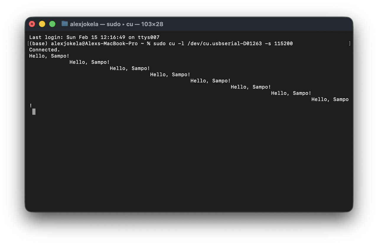
With the corrected patcher, the "Hello, Sampo!" program finally works on the FPGA - looping cleanly with zero character loss:
The Testbench: Trusting but Verifying
One important discovery during this process: the simulation testbench had tx_ready = 1 permanently. The simulated UART never pushed back on the CPU - it accepted every byte instantly. This meant the CPU's busy-wait loop (INI R6, ACIA_STATUS / ADDI R7, -2 / BNE wait) was never actually tested in simulation. The status register always returned "ready," so the loop body executed zero times.
On real hardware, the UART transmitter takes about 87 microseconds per byte at 115200 baud. The busy-wait loop runs hundreds of times per character, exercising the INI instruction, the AND/ADDI flag-setting sequence, and the BNE branch in a tight loop. If any of those instructions had a subtle bug, it would only manifest on hardware.
We added realistic UART timing to the testbench:
parameter TX_BYTE_CYCLES = 108 * 10;  // ~1080 cycles per byte
reg [15:0] tx_delay_cnt;

always @(posedge clk) begin
    if (tx_valid && tx_ready) begin
        tx_ready <= 0;
        tx_delay_cnt <= TX_BYTE_CYCLES;
    end else if (tx_delay_cnt > 0) begin
        tx_delay_cnt <= tx_delay_cnt - 1;
        if (tx_delay_cnt == 1)
            tx_ready <= 1;
    end
end
With this change, simulation exercises the same code paths as the hardware. All 132 tests still pass - the UART flow control logic was correct all along, it just wasn't being tested.
Running All Tests on the FPGA
With the patch bug fixed, we ran the complete suite. Each test requires a separate FPGA build (Yosys synthesis, nextpnr place-and-route, ecppack bitstream generation), programming via JTAG, and serial capture. The Makefile automates the entire pipeline:
fpga-%: $(BUILD_DIR)/sampo_%.bit
    openFPGALoader -b ulx3s $<
    sleep 1
    python3 fpga_capture.py $(SERIAL_PORT) $(SERIAL_BAUD) 5
The fpga_capture.py script opens the serial port, discards the first partial iteration (we might join mid-stream), waits for the === ... === header line that starts each test, captures everything until the header repeats, and outputs one clean iteration.
The results:
========================================
=== FPGA: test_alu ===
========================================
=== ALU Tests ===
ADD basic: PASS
ADD zero: PASS
ADD carry out: PASS
...
AND clr C/V: PASS
All tests passed!

========================================
=== FPGA: test_addi ===
========================================
...
All tests passed!

...

========================================
FPGA Test Summary: 10 passed, 0 failed
========================================
All 10 test suites pass. All 132 individual tests pass. Zero failures on real hardware.
| Test Suite | Tests | FPGA Result |
|---|---|---|
| ALU (ADD, SUB, AND, OR, XOR) | 20 | All PASS |
| ADDI (immediate arithmetic) | 10 | All PASS |
| Shift (SLL, SRL, SRA, ROL, SWAP) | 17 | All PASS |
| MulDiv (MUL, DIV, REM variants) | 12 | All PASS |
| Load/Store (LW, LB, LBU, SW, SB) | 11 | All PASS |
| Branch (all 16 conditions) | 24 | All PASS |
| Jump (J, JR, JALR, JX, JALX) | 6 | All PASS |
| Stack (PUSH, POP, CMP, TEST, MOV) | 12 | All PASS |
| Misc (EXX, GETF, SETF, SCF, CCF, NOP) | 9 | All PASS |
| Extended (ADDIX, SUBIX, SLLX, etc.) | 11 | All PASS |
| Total | 132 | All PASS |
What This Means
Having all 132 ISA tests pass on hardware is a significant milestone for the project. It means:
The Verilog RTL is correct. Every instruction in the Sampo ISA produces the right result, sets the right flags, and handles edge cases (zero, overflow, carry, sign extension) correctly. Not just in behavioral simulation, but in synthesized logic on a real FPGA running at 12.5 MHz.
The assembler is correct. All 66 instructions encode properly. Branch offsets calculate correctly. Extended instructions (LIX, JALX, OUTX) with their 32-bit encoding work. The sasm Rust assembler and the Verilog decoder agree on every instruction format.
The LLVM backend has a solid foundation. When the Rust compiler generates a ADD or BNE or JALX, the hardware will execute it correctly. The test suite doesn't exercise every possible code generation pattern, but it validates every primitive instruction that the compiler builds upon.
The UART subsystem works end-to-end. Status register polling, TX busy-wait, byte transmission, baud rate generation - all verified on hardware. The MC6850-compatible interface works exactly as specified.
Lessons Learned
Test your assumptions. The testbench had tx_ready = 1. It went unnoticed because simulation "worked." The real hardware exercises code paths that simulation shortcuts. Add realistic peripheral timing to your testbenches from day one.
Binary patching is fragile. Inserting bytes into a binary without updating references is a classic relocation bug - the same class of problem that linkers exist to solve. If your patch changes the size of anything, every address reference past the patch point is wrong. The fix - placing the patch in unused address space and using a same-size replacement instruction - avoids the problem entirely.
Simulation is necessary but not sufficient. The pipeline hazard bug was caught by simulation. The address shift bug was invisible to simulation (both used the same patching script, and the original programs - without patching - worked fine). You need both simulation and hardware testing, exercising different code paths and different failure modes.
Systematic testing finds bugs that demos don't. "Hello, Sampo!" worked on the FPGA from day one. It exercises LIX, LBU, CMP, BEQ, INI, OUTI, ADDI, and J - about 8 instructions. The pipeline hazard only manifested when a store was followed by a load to a different address, a pattern that doesn't occur in a simple print loop. You need tests specifically designed to exercise corner cases.
What's Next
The entire Sampo project - assembler, emulator, Verilog RTL, FPGA build scripts, test suite, and LLVM backend - is open source on GitHub. With hardware verification complete, the next steps might be:
-
Running Rust-compiled code on the FPGA. The LLVM backend generates assembly, the assembler produces hex files, and we now know the hardware executes them correctly. Closing this loop -
cargo buildto blinking LEDs - is the obvious next milestone. - Adding more peripherals. The ULX3S has 32MB of SDRAM, an HDMI output, a microSD slot, and an ESP32 co-processor. Each of these opens up interesting possibilities for a working 16-bit computer.
- Performance optimization. The CPU currently runs at 12.5 MHz with a multi-cycle FSM (5-8 cycles per instruction). Pipelining could push this significantly higher on the ECP5.
But first: 132 tests, zero failures. The Sampo CPU works.
This is Part 4 of the Sampo series. Part 1 covers architecture design, Part 2 covers FPGA implementation, and Part 3 covers the LLVM backend.
Recommended Resources
- OrangeCrab ECP5 FPGA Board - A compact Lattice ECP5 board with DDR3 and USB-C, available on Amazon
- ECP5 FPGA Development Boards - Other ECP5 boards available on Amazon
- Getting Started with FPGAs by Russell Merrick - Beginner-friendly introduction with Verilog and VHDL examples
- FTDI USB Serial Adapters - Useful for UART debugging with FPGAs
- USB Logic Analyzers - Essential for debugging digital signals
Source Code
- github.com/ajokela/sampo - CPU architecture, assembler, emulator, Verilog RTL, test suite, and FPGA build scripts
- github.com/ajokela/llvm-sampo - LLVM backend and Rust target specification