The RetroShield Z80 by Erturk Kocalar at 8bitforce.com is one of my favorite pieces of hardware. A real Zilog Z80 CPU on a shield that plugs into an Arduino Mega. The Arduino emulates memory and I/O while the Z80 executes real instructions on real silicon. I've used it to boot CP/M, play Zork over WiFi, port it to the Arduino Giga R1, and even commission a custom level-converter shield to bridge the voltage gap.
But a single Z80 is, well, a single Z80. Real multi-processor Z80 systems existed in the 1980s. Machines like the Cromemco System Three and some S-100 configurations ran multiple Z80s on a shared bus, with bus arbitration mediating access. The question that kept nagging at me: could I fit a second Z80 onto the RetroShield?
I should be honest about something: PCB design is one of my least knowledgeable areas of computing. I'm comfortable with firmware, with compilers, with operating systems, but the physical layer, the world of copper traces and drill files and design rule checks, is territory I've mostly avoided. I can read a schematic, but I've never designed a board from scratch. What I wanted to find out was whether modern AI tools could bridge that gap, whether I could use AI to help me understand, alter, and extend Erturk Kocalar's existing RetroShield design into something new without becoming a PCB design expert first.
This is part one of a two-part series. This piece covers the design: architecture decisions, schematic work, PCB layout, autorouting, and Gerber generation. Part two will cover the physical boards arriving from the fab, assembly, bring-up, and the firmware that makes two Z80s cooperate.
One more thing worth mentioning up front: every step of this design was done without a GUI. That was intentional. I wanted to see how far I could get with just a terminal, command-line EDA tools, AI assistance, and Python scripts that modify PCB files directly. Partly because I think text-based workflows compose better with AI; it's much easier for an AI to generate a Python script that manipulates a text-based PCB file than to drive a graphical EDA tool. And partly because I wanted the entire process to be reproducible and scriptable, not trapped in a series of mouse clicks I'd never remember.
The Original Design
The stock RetroShield Z80 is a clean, simple board. A 55.88mm × 53.34mm two-layer PCB carrying:
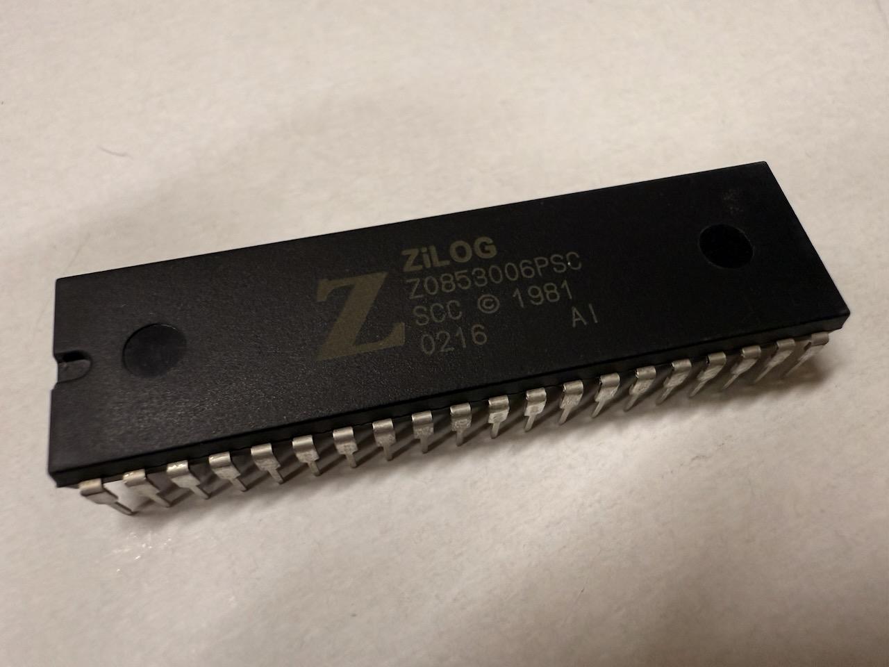
- U1: A Z80 CPU in a DIP-40 package
- J1: A 2×18 pin header (36 pins) that plugs into Arduino Mega 2560 pins 22–53
- A handful of passives: decoupling caps (C1, C2), a clock cap (C3), a clock series resistor (R1), an LED current-limiting resistor (R3), and a bus activity LED
The J1 header carries everything the Z80 needs: 16 address lines (A0–A15), 8 data lines (D0–D7), and control signals (CLK, RESET, INT, NMI, MREQ, IORQ, RD, WR). The Arduino drives the clock, provides the data when the Z80 reads, captures the data when the Z80 writes, and emulates whatever memory and I/O map you define in firmware. It's elegant in its simplicity; the Z80 thinks it's talking to a real computer, and in a sense, it is.
The schematic and PCB files use the gEDA format, text-based files that are human-readable and, crucially, scriptable. The schematic (.sch) defines the logical connections. The PCB (.pcb) defines the physical layout: component footprints, copper traces, vias, and board outline. Both are just text. This matters a lot for what comes next.
Why Two Z80s?
The honest answer is that I wanted to see if it could be done. But there are genuinely interesting things you can do with two processors sharing a bus:
Asymmetric multiprocessing. One Z80 runs CP/M as the primary CPU. The second handles I/O (serial communication, disk access, network operations), freeing the primary CPU from waiting on slow peripherals. This mirrors how some S-100 systems used coprocessor boards.
Cooperative multitasking. Both CPUs execute independent programs, taking turns on the shared bus. The Arduino arbitrates access using the Z80's built-in BUSRQ/BUSACK mechanism, a hardware handshake designed exactly for this purpose. One CPU gets the bus, executes for a while, then yields so the other can run.
Debugging and instrumentation. The second CPU can monitor the first. Watch the address bus to trace execution. Compare outputs. Run the same code on both CPUs and verify they produce identical results, which is useful for testing Z80 clones or FPGA implementations against real silicon.
The Z80 was designed for multiprocessor operation. As Rodnay Zaks details in Programming the Z80, it has dedicated bus request (BUSRQ) and bus acknowledge (BUSAK) pins specifically for multi-master bus sharing. Steve Ciarcia's Build Your Own Z80 Computer covers the hardware side of these signals in practical detail. Most hobbyist projects never use them. This one does.
Architecture: Shared Bus with Independent Control
The first design I considered (and quickly rejected) gave each Z80 its own independent header. Two 36-pin headers, two complete sets of address, data, and control lines. This would have worked electrically, but it was wrong for several reasons. It would have required either two Arduino Megas or consumed all the I/O on one Mega with nothing left for bus arbitration. The board would have been enormous. And it wouldn't have reflected how real multi-processor Z80 systems actually worked.
The right approach is a shared bus. Both Z80s connect to the same address and data lines through J1. They take turns driving the bus, just like in a real S-100 system. What each CPU needs independently is its own set of control signals: its own clock, its own reset, its own interrupt lines, and its own bus request/acknowledge pair.
I checked the Arduino Mega's pin budget. J1 uses pins 22–53 (32 I/O pins). The Mega still has pins 2–21 (20 pins) plus analog pins A0–A15 (16 more, usable as digital I/O), leaving 36 pins sitting idle. A second CPU's control signals only need about 10 pins. There was plenty of room.
The solution: a small supplementary 2×6 header (J2, 12 pins) carrying CPU2's independent control signals to the Arduino's remaining pins:
Pin 1:  +5V         Pin 2:  GND
Pin 3:  CLK_2       Pin 4:  RESET_2
Pin 5:  INT_2       Pin 6:  NMI_2
Pin 7:  MREQ_2      Pin 8:  IORQ_2
Pin 9:  RD_2        Pin 10: WR_2
Pin 11: BUSRQ_2     Pin 12: BUSAK_2
BUSRQ and BUSAK are the key pins. The Arduino firmware pulls BUSRQ low on whichever CPU should yield the bus. That CPU finishes its current machine cycle, tristates its outputs, and asserts BUSAK to signal it's off the bus. The other CPU can then drive the bus freely. It's the same mechanism Zilog designed in 1976; I'm just finally using it.
Building the Schematic, Without a Schematic Editor
The original project used classic gEDA tools (gschem, pcb), which are no longer packaged for Ubuntu 24.04. The modern replacement is lepton-eda, a maintained fork that reads the same file formats. But since the whole point was to avoid a GUI, even lepton-schematic's graphical mode was off the table.
This is where AI earned its keep. I don't have the gEDA file format memorized; I've never needed to. But AI can work through the format specification and generate correct output. I described what I wanted (a second Z80 sharing the existing bus, with independent control signals on a new header), and the AI helped me produce the schematic files, the symbol definitions, and eventually the PCB modifications. I still had to understand the architecture and make the design decisions, but the AI handled the translation from intent to file format.
gEDA schematic files are text. A component placement looks like this:
C 44300 47700 1 0 0 z80-1.sym
{
T 44400 59000 5 10 1 1 0 0 1
refdes=U2
}
That's a Z80 symbol placed at coordinates (44300, 47700), with reference designator U2. Net connections are similarly textual. N entries define wire segments, U entries define bus rippers. You can write an entire schematic in a text editor if you understand the coordinate system.
I created a new schematic page, kz80_cpu2.sch, for the second CPU. In gEDA's multi-page scheme, nets with the same name on different pages are automatically connected. So CPU2's address pins connect to nets named A0, A1, ..., A15 (the same net names used on page 1), and the netlister merges them into shared nets. The shared bus happens at the netlist level without any explicit cross-page wiring.
The one component that didn't exist yet was the 2×6 control header. I wrote a new gEDA symbol file (ctrlhdr2x6-1.sym) from scratch, a rectangular body with 12 pins, labeled with the control signal names, specifying the HEADER12_1 footprint. It's about 30 lines of text, all hand-written.
CPU2's schematic connections break down cleanly:
Shared with CPU1 (same net names, auto-merged): A0–A15, D0–D7, +5V, GND
Independent to CPU2 (new nets with _2 suffix): CLK_2, RESET_2, INT_2, NMI_2, MREQ_2, IORQ_2, RD_2, WR_2, BUSRQ_2, BUSAK_2
The total net count went from 37 to 48, only 11 new nets for an entirely new processor. That's the elegance of the shared-bus approach.
Modifying the PCB With Python
Here's where the CLI-only constraint got interesting. The normal workflow would be: run lepton-sch2pcb to update the PCB with new components from the schematic, then open the PCB in a graphical editor to place and route them. But lepton-sch2pcb had trouble finding footprints in pcb-rnd's library paths, and I didn't have a graphical editor anyway.
So I had AI write a Python script (add_cpu2_shared.py) to modify the PCB file directly. The pcb-rnd file format is text-based, with clearly delimited blocks for each component (Element), each copper trace (Line), each via (Via), and the netlist (NetList). The script:
Widened the board from 55.88mm to 86.36mm, an extra 30.48mm to accommodate the second Z80 and control header, placed on the right half of the board.
Inserted five new Element blocks: U2 (Z80, DIP-40), J2 (2×6 header), C4 and C5 (decoupling and clock caps), and R2 (clock series resistor). Each Element block is essentially a footprint definition: pin positions, pad dimensions, drill sizes, silkscreen outlines. I copied the dimensional parameters from the existing components to maintain consistency.
Updated the netlist in two ways. For shared nets (A0–A15, D0–D7, +5V, GND), the script found each existing net block and appended Connect("U2-xx") entries. For CPU2's independent control signals, it created 11 entirely new net blocks. The +5V net picked up four new connections: U2's VCC pin, U2's WAIT pin (tied high, since WAIT is active low, so high means "not waiting"), C4, and J2.
The result was a valid PCB file with all components placed and all nets defined, but no copper traces connecting anything.
Autorouting: Let the Machine Do the Tedious Part
With components placed and nets defined, the board needed routing: actual copper traces connecting all those pins. Doing this by hand over SSH would have been masochistic. This is exactly what autorouters exist for.
The workflow: export the PCB to Specctra DSN format (an industry-standard interchange format for autorouters), run Freerouting, then import the results back.
First Attempt (Failed)
The first attempt exported the PCB with the original CPU1 traces still in place, hoping Freerouting would preserve them and only route the new nets. Instead, Freerouting spent 50+ seconds per pass trying to work around traces it couldn't associate with its own net encoding. After 48 passes and 40 minutes, it was still failing to route several nets.
Second Attempt (Clean Slate)
Another AI-generated Python script (strip_traces.py) removed all existing copper traces from the PCB file. This was a careful operation. The script had to remove Line[...] entries inside Layer blocks (copper traces) while preserving ElementLine[...] entries (component silkscreen outlines that look syntactically similar).
With a clean board, Freerouting ran in headless mode:
java -jar /tmp/freerouting.jar -de kz80.dsn -do kz80.ses -mp 20
It completed the initial routing in 10 passes, then spent another 49 passes optimizing trace length, converging at pass 59 with the message: "There were only 10.60 track length increase in the last 5 passes, so it's very likely that autorouter can't improve the result further."
Total routing time: about three minutes. The result: 191 wires decomposed into 897 individual trace segments, plus 82 vias for layer transitions. Every net connected. Every design rule satisfied.
Importing Routes Back
One more headless problem: pcb-rnd's SES import requires the GUI. I tried xvfb-run with action commands, but it hung waiting for GTK widget interactions that couldn't happen without a display.
The solution was yet another AI-generated Python script (ses_to_pcb.py) that parsed the Freerouting SES output and injected the routes directly into the PCB file as copper Line entries. The main complication was coordinate system conversion: the SES file uses a bottom-left origin (y increases upward) while pcb-rnd uses a top-left origin (y increases downward). The script also handled via translation, mapping Freerouting's via definitions to pcb-rnd's format with appropriate pad sizes, drill diameters, and clearances.
897 trace segments and 82 vias injected. The PCB was fully routed.
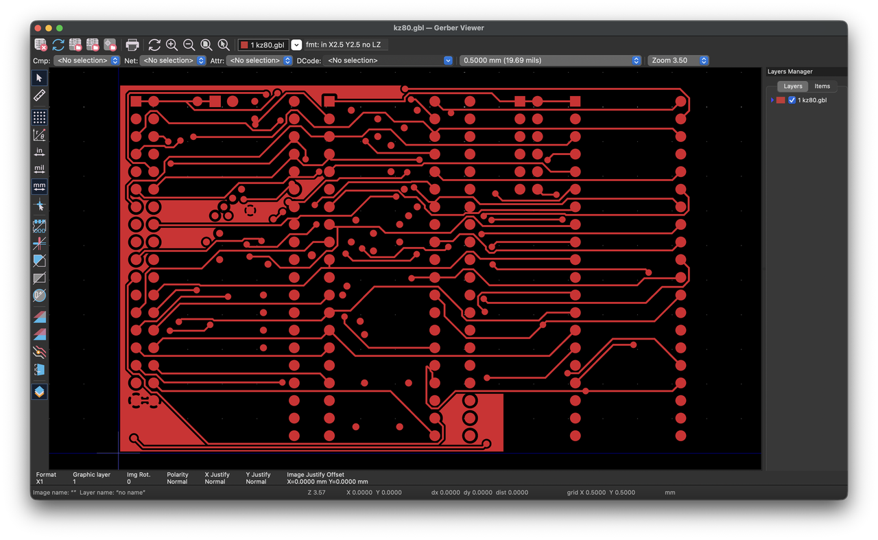
The top copper layer after Freerouting: 897 trace segments connecting 48 nets across both Z80s, the J1 bus header, and the J2 control header. Every trace was placed by the autorouter; none were drawn by hand.
Generating Production Files
The final step was generating Gerber files, the industry-standard format that PCB fabrication houses use to manufacture boards. pcb-rnd's command-line exporter handled this cleanly:
pcb-rnd -x gerber --all-layers kz80.pcb
This produced 11 files covering top and bottom copper, solder mask, silkscreen, paste stencil, board outline, and drill locations. pcb-rnd uses verbose filenames (kz80.top.copper.none.3.gbr), so a renaming script converted them to the standard extensions (.gtl, .gbl, .gts, etc.) that fabrication houses expect.
I also added tinycomputers.io to the top silkscreen layer, placed directly below the existing www.8bitforce.com text, a small nod to both projects.
The final Gerber package: 35KB zipped, ready for fabrication.
The Final Board
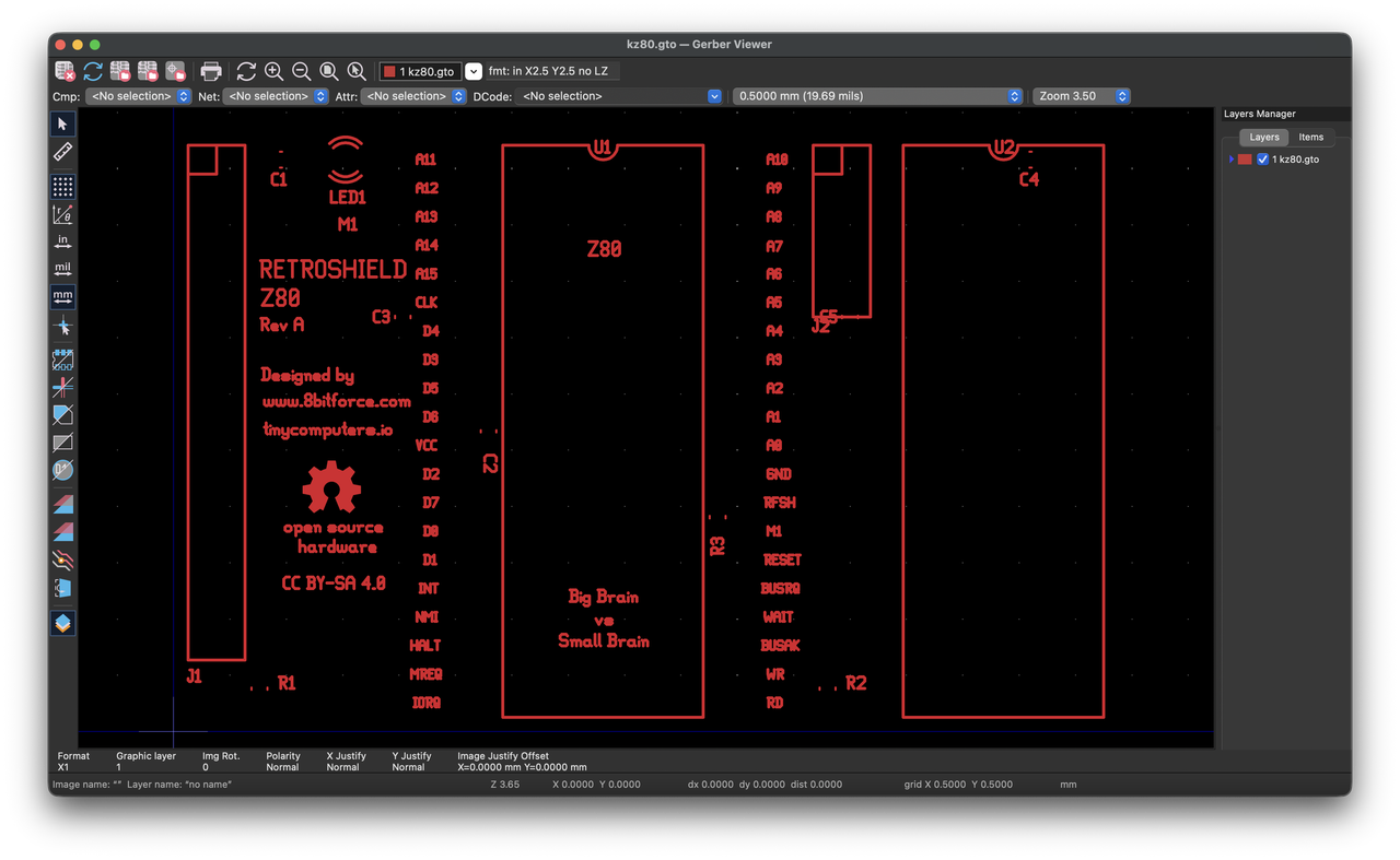
The top silkscreen: U1 (left) and U2 (right) with the J1 bus header on the far left and the J2 control header between the two CPUs. The silkscreen includes the original 8bitforce.com credit alongside tinycomputers.io.
Here's what changed from the original RetroShield to the dual-CPU version:
| Parameter | Original | Dual CPU |
|---|---|---|
| Board dimensions | 55.88 × 53.34mm | 86.36 × 53.34mm |
| Layers | 2 | 2 |
| Z80 CPUs | 1 | 2 |
| Headers | J1 (36 pins) | J1 (36) + J2 (12) = 48 pins |
| Nets | 37 | 48 |
| Through-hole components | 2 | 4 |
| SMD components | 6 | 9 |
| Trace segments | - | 897 |
| Vias | - | 82 |
The board is wider but not taller. The second Z80 sits to the right of the first, with the J2 control header between them. Both CPUs share the J1 bus connection, and the Arduino firmware will manage who drives the bus at any given moment.
The Toolchain Nobody Uses
It's worth stepping back to note what just happened. An entire PCB was designed (schematic capture, component placement, autorouting, Gerber generation) without opening a single graphical application. Every step was either a command-line tool invocation or an AI-generated Python script manipulating text files. And it was done by someone who, at the start of the project, couldn't have told you the difference between a Gerber file and a drill file.
That was the whole point. I chose to avoid a GUI specifically because I wanted to test a hypothesis: that AI-assisted, text-based workflows could let someone with domain knowledge in adjacent areas (firmware, systems programming) operate effectively in an unfamiliar domain (PCB design). The text-based EDA formats made this possible; they gave the AI something it could read, reason about, and generate. A graphical tool would have put me back to square one, clicking through menus I didn't understand.
I'm not claiming this is better than using KiCad or Altium with a mouse. For complex boards with hundreds of components, graphical tools and experienced designers are indispensable. But for a modification like this (adding a known set of components to an existing, well-documented open-source design), AI plus text-based tools was surprisingly effective. I brought the architectural understanding (how Z80 bus arbitration works, which signals need to be shared versus independent) and the AI handled the translation into file formats I'd never touched before. Most of the time was spent understanding the design, not fighting tools.
What's Next
The Gerber files are at the fab now. In part two, I'll cover what happens when the physical boards arrive: inspection, assembly, first power-on, and the Arduino firmware that orchestrates two Z80s on a shared bus. The firmware is where the real complexity lives: bus arbitration timing, memory mapping for two independent address spaces, and the question of what to actually run on a dual-Z80 system in 2026.
Here's a preview of what the bus arbitration core looks like. The Arduino manages which CPU owns the shared bus at any given moment using the Z80's hardware BUSRQ/BUSAK handshake:
// --- Pin definitions (active low) ---
// CPU1 control (directly from J1 via existing RetroShield mapping)
#define CPU1_CLK      A5
#define CPU1_BUSRQ    A4    // directly from Arduino to CPU1 BUSRQ pin
#define CPU1_BUSAK    A3    // directly from CPU1 BUSAK pin to Arduino

// CPU2 control (directly from J2 header)
#define CPU2_CLK      2
#define CPU2_BUSRQ    3
#define CPU2_BUSAK    4

// Bus state
volatile uint8_t active_cpu = 1;

void setup() {
  // BUSRQ is output (Arduino tells CPU to release bus)
  pinMode(CPU1_BUSRQ, OUTPUT);
  pinMode(CPU2_BUSRQ, OUTPUT);

  // BUSAK is input (CPU tells Arduino it released bus)
  pinMode(CPU1_BUSAK, INPUT_PULLUP);
  pinMode(CPU2_BUSAK, INPUT_PULLUP);

  // Start with CPU1 active, CPU2 off the bus
  digitalWrite(CPU1_BUSRQ, HIGH);   // HIGH = don't request bus release
  digitalWrite(CPU2_BUSRQ, LOW);    // LOW  = request CPU2 to release bus
  active_cpu = 1;

  // Wait for CPU2 to acknowledge it's off the bus
  while (digitalRead(CPU2_BUSAK) == HIGH);
}

bool switch_to_cpu(uint8_t cpu) {
  if (cpu == active_cpu) return true;

  uint8_t old_busrq = (active_cpu == 1) ? CPU1_BUSRQ : CPU2_BUSRQ;
  uint8_t old_busak = (active_cpu == 1) ? CPU1_BUSAK : CPU2_BUSAK;
  uint8_t new_busrq = (cpu == 1) ? CPU1_BUSRQ : CPU2_BUSRQ;

  // Ask the active CPU to release the bus
  digitalWrite(old_busrq, LOW);

  // Wait for acknowledgment (CPU finishes current machine cycle first)
  unsigned long timeout = micros() + 1000;
  while (digitalRead(old_busak) == HIGH) {
    if (micros() > timeout) return false;   // hung CPU — shouldn't happen
  }

  // Bus is free. Release the new CPU onto it.
  digitalWrite(new_busrq, HIGH);
  active_cpu = cpu;
  return true;
}
The critical detail is timing. When the Arduino pulls BUSRQ low, the Z80 doesn't stop immediately; it finishes its current machine cycle, which can take 3–6 clock periods depending on the instruction. Only then does it tristate its address, data, and control outputs and assert BUSAK. The while loop waits for that handshake to complete. During the transition, neither CPU is driving the bus, and the Arduino must not attempt any bus operations.
This is a simplified version. The full firmware in part two will handle clock generation for both CPUs, memory mapping, I/O dispatch, and the arbitration policy (round-robin, priority-based, or cooperative yield). But the handshake above is the foundation everything else builds on. It's the same protocol that made multi-Z80 S-100 systems work in the early 1980s.
The hardware design is the easy part. Making two 50-year-old processors cooperate is the challenge.
Source Files
All schematics, PCB files, Gerber outputs, and helper scripts for this project are open source:
- dual-z80: KiCad/gEDA source files, Gerber package, Python scripts for PCB manipulation, and build log
This is part one of a two-part series. Part two will cover board assembly, bring-up, and dual-CPU firmware.
Previous RetroShield posts: CP/M on the RetroShield · Fiverr PCB Design · CP/M on the Giga R1 · Zork on the Giga