The GigaShield boards discussed in this post were fabricated by PCBWay. Their DFM review caught the clearance issue that forms most of this story's middle act — which, as it turns out, is exactly the right kind of thing to catch before the copper is cut. PCBWay offers PCB prototyping, assembly, CNC machining, and 3D printing services with turnaround times starting at 24 hours. pcbway.com.
This is the fourth post in a running series about designing a level-shifter shield for the Arduino Giga R1 using Claude Code and open-source command-line EDA tools. A brief map of what's come before, since the series grew past its original planned scope:
- Fiverr PCB Design (\$468) — the first GigaShield, designed by a freelance contractor in KiCad. It worked for most things but broke against the Z80's tri-state bus because the auto-sensing level shifters couldn't cope with floating signals.
- Redesigning a PCB with Claude Code and Open-Source EDA Tools (Part 1) — the v0.2 redesign. Replaced the TXB0108 auto-sensing shifters with SN74LVC8T245 driven shifters, generated the PCB programmatically from a Python script, autorouted, and shipped Gerbers to fabrication. (The "Part 1" in its title was meant to lead directly into a Part 2 about assembly and bring-up — but a bug derailed that plan.)
- How a Pin Numbering Bug Killed a PCB — the unplanned post-mortem on why the v0.3 board didn't work. A pin-numbering convention mismatch on the dual-row headers put every signal at the wrong physical position. The fabricated board was perfect; the design was wrong.
This post is about the v0.4 respin. It is also an honest accounting of what AI-assisted PCB design actually looks like in practice: the places where the workflow is miraculous, the places where it is agonizing, and the hour-long arguments between Freerouting and pcb-rnd about whether two pieces of copper were three tenths of a millimeter apart.
If you came here looking for a triumphant "I built a PCB with AI and it just worked" story, this is not that post. If you came here looking for a nuanced report from someone who spent days on this and now has calibrated opinions about where it's worth doing, welcome.
The Setup, Briefly
For readers who haven't read the earlier posts: the GigaShield is a 155mm x 90mm PCB that sits between an Arduino Giga R1 (3.3V logic) and a RetroShield Z80 (5V logic). It has ten SN74LVC8T245PW level-shifter ICs translating 72 channels between the two voltage domains. The Giga plugs into the bottom (3.3V headers), the RetroShield plugs into the top (5V headers), and the shifters bridge the two. Our first design used TXB0108 level-shifter ICs but the autosensing signal direction did not play nicely with the Z80's tri-state signals.
The entire PCB is generated by a Python script. Not the schematic — there is no schematic. Not the layout — there is no graphical layout. The script emits a pcb-rnd board file directly: component placements, pad definitions, netlist, board outline, silkscreen text, all in text format. Running python3 build_giga_shield.py produces giga_shield.pcb in a fraction of a second. The board is then routed by Freerouting and exported to Gerbers via pcb-rnd's command-line tools.
Everything happens in the terminal. No GUIs, no mouse clicks, no "did I save the layout?" anxiety.
The v0.3 board — subject of the previous post — failed because of a subtle bug in this pipeline. The v0.4 board fixes that bug and several others I didn't know about. This post covers what it took to find and fix them.
Bug Class #1: The Kind AI Caught Easily
Before refabricating, I asked Claude Code to audit the Python generator for any additional bugs. I framed it as a careful code review with specific checkpoints: pin numbering in both the pcb-rnd and KiCad generators, SN74LVC8T245 pin mapping against the TI datasheet, critical Z80 signal routing, and component placement validation.
The audit took maybe fifteen minutes of wall-clock time — during which Claude Code read the entire codebase, cross-referenced it against the datasheet, and produced a severity-graded report. Most findings were cosmetic (stale comments, a print statement that said "1x10 header" for an 11-pin connector, harmless inconsistencies between the two build scripts). One finding was genuinely important:
H1 — Comment "default A→B" is factually wrong, and U10's pulldown produces incorrect default behavior without user intervention.
DIR=LOW per the SN74LVC8T245 datasheet means B→A (B-side drives A-side). The comment states the opposite. More importantly, U10 uses DIR for CLK, RESET, INT, NMI — signals that must flow A→B (Giga→Z80). With R10 pulling DIR_U10 to GND, U10 powers up in the B→A direction, which means the 5V Z80 side would drive the 3.3V Giga side on these control pins. Backwards and potentially damaging if the Z80 is outputting signals while the Giga is also driving those pins.
This bug is worth dwelling on, because it highlights something important about how I've been working on this project. I didn't write that code. Claude Code did, three weeks earlier, as part of the initial generator script. The wrong comment and the wrong pulldown direction were both introduced by the same LLM that later caught the mistake on audit.
That sounds like it should be embarrassing for the workflow — the tool that generates bugs is also the tool that reviews them — but I think it's actually the right shape of the argument. A single LLM pass is fallible. A single human pass is also fallible. What matters is whether the combined system catches bugs reliably before they ship. In this case, the first pass (generation) introduced a subtle error, the second pass (audit, explicitly framed as a datasheet-cross-referencing review) caught it. The human's job was to know that the second pass was worth requesting — and to recognize, when the audit report came back, which findings mattered and which were cosmetic.
This is exactly the kind of bug that a human engineer might catch on a good day and miss on a bad day. The comment and the circuit were internally consistent but both wrong. The datasheet was authoritative but three hundred pages away. Claude Code's audit didn't find it by being clever — it found it by mechanically cross-referencing every pin mapping against the datasheet, every comment against the actual behavior, with the patience of a machine that doesn't get bored.
The fix was a one-line change: swap R10 from a pulldown-to-GND to a pullup-to-+3V3. U10 now powers up in the correct direction without any firmware intervention.
I'll be transparent: the wrong direction would not have destroyed the boards immediately. The 5V CMOS outputs driving a 3.3V CMOS input is within the chips' absolute maximum ratings for short periods, especially if the Giga's pins are configured as inputs during that window. But in the steady state, with the Arduino trying to drive those pins as outputs, you'd have a lot of current flowing through ESD diodes, probably latch-up, almost certainly failure. A bug that would have cooked several \$70 Arduino Giga R1s over the life of the project.
Fifteen minutes of LLM review. One avoided burn-up. A comfortable argument for the workflow.
Bug Class #2: The Kind AI Didn't Help With At All
Then came the Freerouting clearance saga.
After the v0.4 build script was fixed, regenerated, and re-routed with Freerouting at the familiar 0.254mm trace width and 0.254mm clearance rule, I packaged up the Gerbers and uploaded them to PCBWay. Their automated DFM check failed almost immediately with a message I'd never seen before:
Failed reason: The spacing between copper traces and pads should be larger than 0.1mm.
A few hours later, a QA engineer at PCBWay followed up with a screenshot from their internal Gerber inspection tool. They had loaded the top-copper layer, zoomed into the crowded region around the level-shifter ICs, and drawn yellow arrows at eight or ten spots where traces were running uncomfortably close to pads. At one spot they'd highlighted in cyan, their measurement tool showed D=0 — literal zero distance between a trace and a pad.
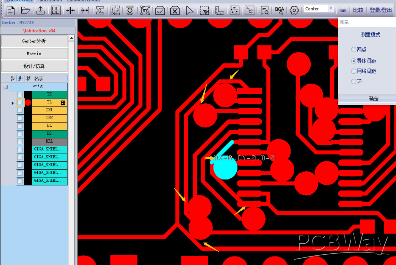
The screenshot PCBWay's QA engineer sent back. Yellow arrows mark the violations. Cyan highlight shows their measurement tool reporting D=0 — a trace touching a pad that it shouldn't be touching.
This should not have been possible. Freerouting had been told to maintain 0.254mm clearance between all copper. 0.254mm is 10 mil, which is more than double PCBWay's 0.1mm minimum. If the router respected its rules, PCBWay's automated check should have sailed through.
But it hadn't.
I went through the usual debugging motions. Ran pcb-rnd's DRC on the routed board: 121 clearance violations. Opened the board in a gerber viewer: confirmed the violations were real, not artifacts. Tightened Freerouting's clearance to 0.3mm, narrowed traces to 0.2mm to give more room, added explicit clearance rules for every object-pair type (wire-pin, wire-via, smd-pin, pin-pin, and so on):
(rule
  (width 0.2)
  (clearance 0.3)
  (clearance 0.3 (type smd_smd))
  (clearance 0.3 (type smd_via))
  (clearance 0.3 (type smd_pin))
  (clearance 0.3 (type pin_pin))
  (clearance 0.3 (type pin_via))
  (clearance 0.3 (type via_via))
  (clearance 0.3 (type wire_wire))
  (clearance 0.3 (type wire_via))
  (clearance 0.3 (type wire_pin))
  (clearance 0.3 (type wire_smd))
)
Re-ran Freerouting. Ninety minutes of autorouting and optimization later, pcb-rnd's DRC still reported 121 clearance violations. Identical count. As if the clearance setting had been ignored entirely.
This went on for several iterations. I tried 0.35mm clearance. 0.4mm clearance. I made the trace narrower. I made it wider. I added explicit rules for each layer. The violation count remained 121. Freerouting's optimization phase consistently took ninety minutes and improved the design by "about 52%" each time. The DRC report was unmoved.
Claude Code was with me through all of this. It read the Freerouting log. It parsed the DRC output. It spotted the p_shape is not bounded warnings (only three occurrences, probably unrelated). It suggested hypotheses — maybe Freerouting measured clearance from via hole centers rather than copper rings, maybe the padstack path shapes were confusing the bounds calculation, maybe pcb-rnd's DRC was using a threshold different from what Freerouting was told. Each hypothesis was plausible. None of them panned out. The violation count stayed at 121.
The breakthrough came not from any clever insight but from a dumb experiment: run the DRC on the unrouted board. Zero violations. Run it after Freerouting: 121 violations. Same 121, every time. Re-route with completely different settings: still 121 violations at roughly the same coordinates.
The coordinates were the tell. The 121 "violations" weren't scattered — they were clustered at specific, consistent locations. And those locations, when I finally examined them carefully, were pin-to-trace junctions. Where a trace ended at a pad on its own net. Where the copper legitimately overlapped because they were the same electrical node.
pcb-rnd's DRC was flagging every legitimate trace-pad connection as a "shorted nets: net too close to other net" violation. Not because the nets were shorted, but because pcb-rnd's DRC algorithm didn't properly account for the fact that two pieces of copper on the same net are supposed to touch. They're supposed to be connected. That's the whole point.
All 121 "violations" were false positives. Freerouting had been maintaining 0.3mm clearance the whole time. pcb-rnd had been lying about it the whole time. And PCBWay's automated DFM had been flagging the real issue — spots where same-net connections appeared to violate clearance under their algorithm — except their tool was smart enough to usually recognize same-net connections, so it flagged only the ones where the overlap happened to look particularly bad in the Gerber rendering.
The fix, once I understood this, was to increase clearance (which I'd been doing) until the visual overlap was conservative enough that PCBWay's tool stopped complaining, and stop trusting pcb-rnd's DRC entirely. The winning configuration was 0.254mm traces with 0.3mm clearance and the explicit per-type clearance rules. PCBWay's DFM passed on that submission.
Total time spent on this: maybe six hours across two days, counting the autorouting time, the iteration loops, and the eventual diagnosis. Nothing Claude Code did made this faster. Claude Code could parse logs and suggest hypotheses as quickly as I could read them, but it couldn't see what I couldn't see. The problem wasn't in any file — it was in the interaction between three tools' different assumptions about what "clearance" means. That kind of bug lives in the interfaces, not in any single artifact. LLMs are not good at debugging interfaces they can't run.
I don't think this is a damning critique of AI-assisted workflows. But it is a calibrating one. If you're choosing between "write a Python script and fight Freerouting and pcb-rnd and PCBWay's DFM" versus "click around in KiCad for four hours," the second path has fewer interfaces to break. Graphical tools eat their own complexity internally. The CLI workflow exposes every seam.
Bug Class #3: The Kind AI Made Worse
At some point during the clearance debugging, I decided to reduce the board from 6 layers to 4 layers. Freerouting had been routing successfully on four, so paying for six was wasteful. I updated the pcb-rnd build script to emit a 4-layer stack, changed the Groups() directive to "1,c:2:3:4,s:5:6:7", regenerated, exported DSN, routed, imported, exported Gerbers.
The resulting Gerber package had five copper layers.
Not six. Not four. Five. With traces scattered across them in a way that suggested pcb-rnd, on SaveTo, had rewritten my Groups() string into something of its own invention — "6:8:1,c:2:3:5:10:11:4,s:9:7" — that created phantom layers and assigned them roles my build script hadn't intended. The gerber named intern.copper.none.12.gbr had 1,406 traces. This was not a layer I had defined.
I asked Claude Code to help me understand pcb-rnd's Groups() syntax. It gamely tried to parse the string. It offered three different interpretations, each of which would have produced a different layer stack than what pcb-rnd actually did. It couldn't fix the problem because it couldn't run pcb-rnd and observe the behavior. I couldn't fix it either, for the same reason with more forgivable excuses.
After maybe two hours of going in circles, I reverted to the original 6-layer Groups() string, re-routed, exported Gerbers (getting six copper gerbers — four with traces, two with only padstack pads), and deleted the two empty ones before zipping. PCBWay doesn't care what my source PCB file says. They fabricate what's in the Gerber bundle. If I submit four copper layers, I get a 4-layer board.
This is a pattern worth noting. Sometimes the right solution to a tool-chain problem isn't to fix the tool chain. It's to work around it. Claude Code is good at helping you solve problems correctly; it's not as good at helping you recognize that the correct solution is to stop trying to solve the problem. That's a uniquely human skill: knowing when to quit.
The Component Placement Lesson
One more story worth telling. The v0.3 design had the ten level-shifter ICs arranged as U1-U5 across the top of the board and U6-U10 stacked in a single vertical column on the right side. It looked tidy. It routed successfully on six layers. It also concentrated an enormous amount of signal traffic into a narrow vertical channel between the shifter cluster and the 2x18 headers — so narrow that Freerouting couldn't route all 308 nets on four layers without leaving some unrouted.
Claude Code flagged this the first time I tried the 4-layer route. Not by proposing a new placement — it didn't. By noting that the unrouted nets all terminated in the same congested region, and asking whether I'd considered spreading U6 through U10 into a staggered two-column layout between J9 and J10. I hadn't. The suggestion was obvious in hindsight, which is the clearest sign that it was useful. A lot of engineering is exactly this: you know the answer once someone mentions it, but no one mentions it and you don't think to ask yourself.
The new placement — U6, U8, U9 in one column closer to J9, U7 and U10 offset in another column closer to J10 — routed cleanly on four layers with 314/314 nets connected. The LLM didn't solve a geometric problem I couldn't solve. It pointed at a geometric problem I hadn't recognized as a problem. That's a different and narrower contribution than "AI designed my board," but it's also real and repeatable.
For the curious: my mental model for why the original layout was bad had been "I want them in a tidy column near the connector." The LLM's implicit mental model, derived from having read every PCB design textbook ever digitized, was "signal traffic wants to spread, not concentrate." Both are defensible. The second is more useful.
What Actually Works
Stepping back from the debugging, here is my honest breakdown of where Claude Code earned its keep on this project versus where it didn't.
Where it was essentially indispensable:
-
Parsing hierarchical S-expression formats. The original KiCad design from the Fiverr engineer was a
.kicad_schfile with nested sheets, positional net labels, and implicit connections across hierarchical boundaries. Extracting the 72-channel signal mapping from that file would have taken me half a day by hand and maybe an hour of Python if I were patient. Claude Code did it in about twenty minutes of interactive conversation. -
Generating boilerplate code with domain-specific constraints. The
tssop24_element()function that produces the SN74LVC8T245PW footprint is three dozen lines of boring arithmetic — pad positions, coordinate transforms, string formatting. I asked for a pcb-rnd Element that matched the SN74LVC8T245PW footprint and got working code on the first try — Claude Code fetched the TI datasheet, read the pcb-rnd format reference, and produced the correct geometry without me having to hand it either document. I would have gotten it wrong on the first try if I'd written it by hand, because I would have flipped the B-side pin order (pins 13-24 run bottom-to-top on this package, which is easy to miss). -
Cross-referencing mechanical information against specifications. The audit I mentioned earlier — reading my entire codebase and checking it against the TI datasheet — would have been tedious and error-prone to do manually. Claude Code did it reliably and caught a bug I would have shipped.
-
File format debugging. pcb-rnd's error messages are unhelpful by the standards of modern software. The Specctra DSN format has undocumented quirks. Gerber apertures have version-specific formatting differences. Every time I hit an error I didn't understand, Claude Code could read the file, diff it against a working example, and tell me what was different. This is LLM work at its best — bulk pattern-matching across reference material I don't have memorized.
-
Bridging the SSH workflow. pcb-rnd runs on Linux and I work on a Mac. Half of the pipeline was shell commands to upload files, run pcb-rnd on a remote machine, download results, and iterate. Claude Code managed that SSH shuffle cleanly across hundreds of invocations. Not a hard problem, but a tedious one. Delegating it was valuable.
Where it didn't help:
-
Diagnosing cross-tool interaction bugs. The 121-false-positive clearance saga was a problem that lived between three tools' different mental models. Claude Code could read each tool's output but couldn't run experiments to validate hypotheses. I had to do that myself, slowly.
-
Making placement decisions involving physical intuition. Claude Code helped with the U6-U10 restacking only after I'd ruled out other options. It didn't lead the design choice. For pure physical intuition — "this will be too dense," "this trace will pick up noise from this inductor," "this via is a mechanical weakness" — the LLM was helpful as a second opinion but not a primary source.
-
Knowing when to stop debugging and accept a workaround. When pcb-rnd's
SaveTomangled my layer stack, Claude Code happily kept trying to fix it. It took me longer than it should have to realize the fix was to not useSaveTo. LLMs are optimized for "helpfully continue the task." Human judgment is needed for "recognize the task is wrong."
The Economics
It's fair to ask whether any of this is worth it. I'll try to be honest.
Time invested in the v0.4 respin, from identifying the pin-numbering bug through submitting the second Gerber package:
- Designing the fix: 2 hours (including the code audit that caught R10)
- Regenerating and re-routing: ~4 hours of wall-clock time, mostly Freerouting optimization
- The clearance debugging saga: ~6 hours
- The layer-stack misadventure: ~2 hours
- Documentation, git commits, this blog post: ~4 hours
Total: ~18 hours of my engineering time, plus a lot of Freerouting CPU-hours.
If I had paid a Fiverr freelancer to redo the design in KiCad from scratch, it would have cost about \$400 and taken about a week of wall-clock time. If I had learned KiCad properly and done the layout myself, it would have taken probably 20 to 30 hours for a 314-net 4-layer board, given I've never used KiCad's layout editor seriously. If I had used a commercial autorouter (Altium's, say), I would have paid thousands of dollars in licensing and probably spent 10 hours on the project.
The Python-and-Claude-Code workflow cost me 18 hours of engineering time and the frustration of debugging interactions between three different CLI tools. PCBWay sponsored the fabrication, so the direct cash outlay was zero on this project — but that's an artifact of the sponsorship, not the workflow. A non-sponsored hobbyist running the same pipeline would spend roughly \$50 per prototype fabrication run at PCBWay's standard rates, so two runs (v0.3 plus v0.4) would be in the ballpark of \$100 total. The boards will arrive next week.
Is that a good trade? It depends on what you value. For me, the workflow is repeatable — the next board I design will take a fraction of this effort because the tool chain is now debugged. For someone doing one PCB in their lifetime, this would be a terrible trade. For someone who plans to iterate on a design family over months or years, it's probably a good one. The upfront cost amortizes.
I don't think the right question is "AI-assisted PCB workflow yes or no." I think it's "what kind of PCB work are you doing, and does your workflow compound?" If your boards are one-offs, use KiCad. If your boards are a family that evolves over time, scripted workflows start paying for themselves around the third iteration. Add AI assistance on top and the break-even point moves earlier.
What I'd Do Differently
A few hard-won principles from this project, in case anyone tries something similar:
Validate the pipeline on a dead-simple board before using it for a real one. If I had generated a toy two-net board first, routed it, exported Gerbers, and submitted the files to PCBWay's online DFM check as a dry run, I would have caught the pin-numbering convention bug without wasting a fabrication run on v0.3. The total time for the dry run would have been maybe two hours. It would have saved a two-week turnaround — and, more importantly, not burned a sponsored fabrication run on a design that was never going to work.
Run DRC with multiple tools and compare. pcb-rnd's DRC was actively misleading on this board. If I had also run the Gerbers through a third-party tool like Gerber Viewer or through KiCad's DRC after importing, I'd have noticed the disagreement and dug into it earlier. Never trust a single tool's DRC as authoritative.
Keep PCBWay's DFM as the source of truth. Their automated check has seen more boards than any open-source DRC. It's tuned for actual manufacturability. When the open-source tools say "clean" and PCBWay says "fail," believe PCBWay.
Write test fixtures for the scripted generator. A few unit tests that verify "net X has pins Y and Z" would have caught the pin-numbering bug in the build step rather than the fabrication step. For a scripted PCB workflow, the Python code needs the same test discipline as any other production code.
Budget for LLM's failure modes. The LLM is fast and confident but can spiral into unproductive debugging loops. When a fix doesn't work on the second or third try, that's the signal to stop and think rather than let the LLM keep trying variations. Six hours on the clearance bug should have been two.
The Broader Question
There's a cultural current in software circles right now that frames AI coding assistants as either revolutionary or fraudulent. Neither frame captures what I experienced on this project.
Claude Code didn't replace my expertise. I still had to know what a level shifter is, why the Z80 tri-states its bus during IO cycles, why the annular ring on a via matters for fab yield, when a pull-up is safer than a pull-down. Without that domain knowledge, I couldn't have directed Claude Code at the right problems, and I couldn't have recognized when its suggestions were wrong.
Claude Code also didn't slow me down. The audit that caught the R10 bug was pure leverage. The file-format debugging was pure leverage. The SSH shuffle was pure leverage. The CLI workflow I'm using would not be tractable without an LLM assistant — too many file formats, too many tools, too much boilerplate. Claude Code didn't enable the workflow, but it made it something I could actually use instead of abandoning it for KiCad's GUI after the first pcb-rnd error message.
What Claude Code is, for PCB design, is a competent junior collaborator with encyclopedic memory, infinite patience, and no physical intuition. It won't design your board for you. It'll help you design your board, if you know what you're doing. That's a different and less exciting claim than the marketing suggests, but it's also a more durable one.
What's Next
The v0.4 boards are scheduled to arrive from PCBWay in a few weeks. If they work — if the Z80 actually responds to its clock, if the data bus reads are clean, if /IORQ is no longer stuck at ground — I'll write a Part 4 covering the bring-up and the test results. If they don't work, I'll write a Part 4 about whatever new bug I've introduced.
In the meantime, the Python build script, pcb-rnd source files, Gerber outputs, Arduino test sketch, and every piece of infrastructure discussed in these posts is open source:
- giga-shield — Complete design files, build pipeline, and test firmware
If you're interested in scripted PCB design workflows, I'd genuinely like to hear from people who've tried similar approaches — or, more interestingly, tried and given up. The body of public literature on "I attempted this and it didn't work for me" is much smaller than on "I succeeded, here's how," and I think the former is more useful.
*Previous posts in this series: Redesigning with Claude Code (Part 1) · How a Pin Numbering Bug Killed a PCB · Fiverr PCB Design (\$468)