My [previous CP/M build](/posts/cpm-on-physical-retroshield-z80/) runs great. A real Z80 on a [RetroShield](https://baud.rs/87wbBL), DRAM shield for 64KB, SD card for disk images, all sitting on an [Arduino Mega 2560](https://baud.rs/DzXGr4). It boots CP/M, runs Zork, the works. So naturally I decided to make my life harder.
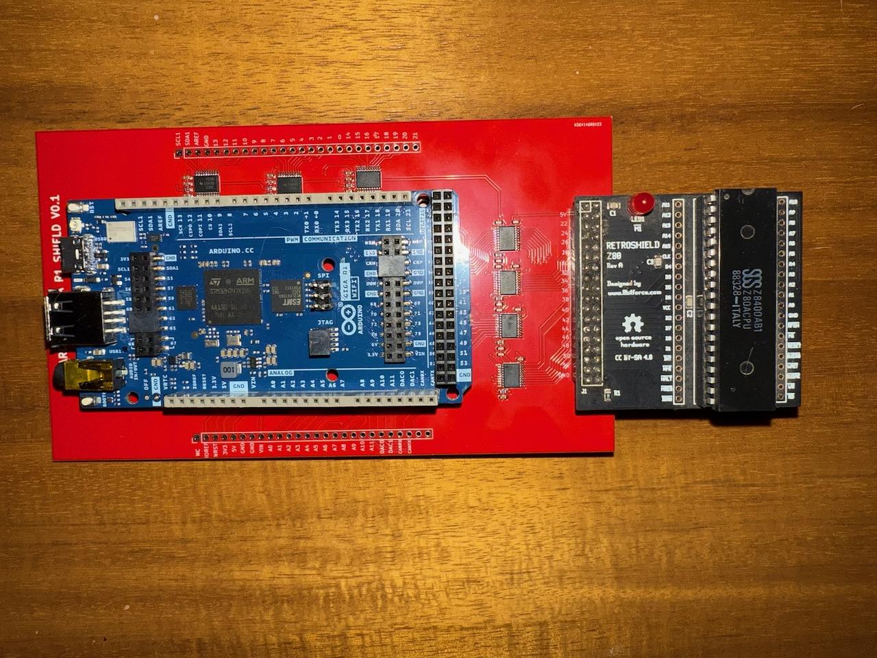 The [Arduino Giga R1 WiFi](https://baud.rs/poSQeo) is a significantly more powerful board: a dual-core STM32H747 running at 480MHz, 1MB of internal SRAM, 8MB of SDRAM, and built-in WiFi. Where the Mega's 16MHz AVR crawled through bus cycles, the Giga could theoretically fly. And all that internal RAM means we can ditch the [KDRAM2560](https://baud.rs/iJn6Sd) DRAM shield entirely — just a 64KB byte array in SRAM.
There was just one problem. The Giga runs at 3.3V logic. The Z80 runs at 5V. And as I'd learn the hard way, bridging that gap would consume more debugging hours than everything else combined.
This post documents the port: the hardware stack, the architectural pivot to WiFi-based disk I/O, the level converter nightmare, the shadow register workaround that saved the project, and the Rust sector server that ties it all together. If you want the backstory on the [custom level converter PCB](/posts/fiverr-pcb-design-arduino-giga-shield/), that's a separate post.
## The Hardware Stack
The upgraded system has fewer physical components than the Mega version, but more going on under the hood.
| Component | Mega Version | Giga Version |
|-----------|-------------|--------------|
| Processor | ATmega2560, 16MHz | STM32H747, 480MHz Cortex-M7 |
| Logic Level | 5V native | 3.3V (needs level converter) |
| Z80 RAM | KDRAM2560 DRAM shield | 64KB byte array in SRAM |
| Bus I/O | AVR port registers (parallel) | digitalRead/Write (per-pin) |
| Disk Storage | SD card (software SPI) | WiFi to sector server |
| Extra Hardware | DRAM shield + SD adapter | Level converter board only |
The RetroShield Z80 plugs in the same way — it uses the same physical pin positions. The level converter board sits between the Giga and the RetroShield, translating all bus signals between 3.3V and 5V. The board uses [TXB0108](https://baud.rs/hY6ydl) bidirectional level converters, which sense the drive direction automatically.
At least, that's what they're supposed to do.
### CP/M Memory Map
The Z80 sees the same 64KB address space as on the Mega:
```
0000-00FF Page Zero (jump vectors, FCBs, command buffer)
0100-DFFF TPA (Transient Program Area) — 56KB
E000-E7FF CCP (Console Command Processor)
E800-F5FF BDOS (Basic Disk Operating System)
F600-FFFF BIOS (Basic I/O System)
```
On the Mega, this lived in the KDRAM2560's dynamic RAM with its complex refresh timing. On the Giga, it's just:
```cpp
byte z80RAM[65536];
```
One line. The Giga's 1MB of internal SRAM makes the entire DRAM shield unnecessary.
## WiFi Instead of SD
The original plan was to keep the SD card. The Mega version used software SPI on pins 4-7 since the RetroShield claims the hardware SPI pins. On the Giga, the RetroShield still claims all 76 digital pins — but this time there are no spare analog pins conveniently routed for software SPI either.
The initial idea was to wire a MicroSD adapter to the analog pins. But that meant more custom wiring on top of the already-custom level converter board. And anyone trying to replicate this project would need to solder yet another adapter.
Then it hit me: the Giga has WiFi built in. Why not serve disk images over the network?
The more I thought about it, the more sense it made:
- **No additional hardware.** WiFi is built into the Giga. Zero extra wiring.
- **Better reproducibility.** The project already requires a custom level converter. Adding another custom wiring job makes it harder for others to build.
- **The sector server is just software.** Anyone can download and run a binary. Compare that to soldering an SD adapter to analog pins.
- **It plays to the Giga's strengths.** If you're upgrading from a Mega, you might as well use what makes the Giga special: WiFi and RAM.
- **Future potential.** The 8MB SDRAM could cache entire disk images downloaded over WiFi at boot. CP/M on a RAM disk — faster than any physical media the Z80 ever had access to.
The tradeoff is that the system is no longer self-contained. It needs a WiFi network and a computer running the sector server. For a project that already requires a custom level converter PCB, this felt acceptable.
## The Level Converter Problem
This is where the project nearly died.
The TXB0108 is a popular bidirectional level converter. It uses auto-direction sensing — whichever side drives a signal stronger "wins," and the converter translates accordingly. This works well for simple I2C and SPI signals where direction is clear.
It does not work well for a Z80 bus.
### Signal-by-Signal Breakdown
I built a pin diagnostic sketch to test each signal through the level converter. Here's what I found:
| Signal | Pin | Expected | Actual | Status |
|--------|-----|----------|--------|--------|
| MREQ_N | 41 | Toggles on memory access | Toggles correctly | Working |
| WR_N | 40 | Toggles on writes | Memory writes only | Partial |
| RD_N | 53 | Toggles on reads | Stuck HIGH always | Broken |
| IORQ_N | 39 | Toggles on I/O access | Stuck HIGH always | Broken |
| Address Bus | 22-37 | 16-bit address | All bits correct | Working |
| Data Bus (A→Z80) | 42-49 | Arduino drives data | Works | Working |
| Data Bus (Z80→A) | 42-49 | Z80 drives data | Memory writes only | Partial |
Two signals completely stuck. Two signals working only half the time. The auto-direction sensing that makes the TXB0108 convenient is exactly what makes it unreliable here — the Z80's bus signals have complex timing relationships where drive strength varies throughout the cycle.
### RD_N: Permanently Stuck
`RD_N` on pin 53 never toggles. It reads HIGH regardless of what the Z80 is doing. Pin 53 is the hardware SPI SCK pin on the Mega, and may have internal pull-ups or other conflicts on the Giga's STM32. Combined with the TXB0108's direction sensing, the signal simply can't get through.
The fix is trivial once you realize it: during any bus cycle, the Z80 is either reading or writing. They're mutually exclusive. So:
```cpp
#define STATE_RD_N (!STATE_WR_N)
```
If `WR_N` isn't asserted, it must be a read. This works for all standard Z80 bus operations.
### IORQ_N: The Big One
`IORQ_N` on pin 39 is also stuck HIGH. This is the signal that tells us the Z80 wants to talk to a peripheral — console I/O, disk I/O, everything. Without it, we have no way to detect I/O operations through the bus.
But we have something the bus doesn't know about: we control the Z80's memory. Every byte the Z80 fetches comes from `z80RAM[]`, which we serve. We can read the opcode stream and know exactly what instruction the Z80 is executing — including `OUT (n), A` (opcode `0xD3`) and `IN A, (n)` (opcode `0xDB`).
So instead of watching for IORQ_N to go low, we watch for the Z80 to fetch an I/O instruction from memory.
### Data Bus: Invisible During I/O OUT
This was the subtlest failure. During `OUT (n), A`, the Z80 puts the A register value on the data bus. We should be able to read it. But we can't.
The TXB0108 latches the last strongly-driven value. Since the Arduino drives the data bus during memory reads (pushing 3.3V through the converter to the Z80's 5V side), the converter's direction gets stuck. When the Z80 tries to drive data back during an I/O write, its 5V output can't overcome the converter's latched direction.
I confirmed this by sampling the data bus at every clock tick during an `OUT` cycle. It showed `0x80` (the last value the Arduino had driven — a port number) at every single tick. Zero variation. The Z80's output was completely invisible.
### WR_N: Only Works Sometimes
`WR_N` toggles correctly during memory write cycles but never during I/O write cycles. The timing or drive strength during I/O is just different enough that the converter can't track it.
This meant we couldn't use WR_N to detect when an I/O write was complete either. Every signal we'd normally use for I/O detection was either stuck or unreliable.
## Shadow Register Tracking
The solution to the data bus problem is to never read the data bus during I/O at all. Instead, we maintain a shadow copy of the Z80's A register by watching the opcode stream.
Since we serve every byte the Z80 reads from `z80RAM[]`, we can decode the instruction stream in real time. When we see `LD A, 0x03` (opcode `0x3E 0x03`), we set `shadowA = 0x03`. When we later see `OUT (0x10), A` (opcode `0xD3 0x10`), we already know A contains `0x03` — no need to read the bus.
### M1 Detection
The first challenge is knowing when the Z80 is fetching an opcode (M1 cycle) versus reading data. We detect M1 by watching for the first MREQ-active read after a MREQ-inactive cycle — the rising-to-falling edge of MREQ activity:
```cpp
bool mreq_active = !digitalRead(uP_MREQ_N);
if (mreq_active && !prevMREQ_active && opcodeSkip == 0) {
uint8_t opcode = z80RAM[uP_ADDR];
// This is an M1 fetch — decode the instruction
}
```
### The opcodeSkip Counter
After M1, the Z80 runs a refresh cycle (which reuses the address bus — when the I register is 0 after reset, refresh addresses overlap with boot code at 0x0000+). If we mistook a refresh cycle for another M1, we'd corrupt the shadow registers by "decoding" whatever data happened to be at the refresh address.
The fix is a 256-entry lookup table that tells us how many MREQ-active read cycles to skip after each opcode:
```cpp
static const uint8_t skipCount[256] = {
// 0x00-0x0F: NOP=1, LD BC,nn=3, ...
1, 3, 1, 1, 1, 1, 2, 1, 1, 1, 2, 1, 1, 1, 2, 1,
// ... 256 entries covering every Z80 opcode
};
```
A 1-byte instruction like `NOP` gets skip=1 (refresh only). A 3-byte instruction like `LD HL, nn` gets skip=3 (refresh + 2 operand reads). I/O instructions get skip=0 because their skipping is handled by the I/O state machine. After each M1, we set `opcodeSkip = skipCount[opcode]` and decrement it on each subsequent MREQ-active read cycle.
### Register Tracking
We don't need to track every Z80 register — just enough to know what value A holds when an `OUT` happens. The BIOS uses a relatively small set of instructions to load registers before I/O:
```cpp
switch (opcode) {
// === IO Instructions ===
case 0xD3: { // OUT (n), A
uint8_t port = z80RAM[uP_ADDR + 1];
handle_io_write(port, shadowA);
break;
}
case 0xDB: { // IN A, (n)
uint8_t port = z80RAM[uP_ADDR + 1];
ioResponse = handle_io_read(port);
shadowA = ioResponse; // IN updates A
break;
}
// === A register tracking ===
case 0x3E: shadowA = z80RAM[uP_ADDR + 1]; break; // LD A, n
case 0xAF: shadowA = 0; break; // XOR A
case 0x79: shadowA = shadowC; break; // LD A, C
case 0x78: shadowA = shadowB; break; // LD A, B
case 0x7C: shadowA = shadowH; break; // LD A, H
case 0x7D: shadowA = shadowL; break; // LD A, L
case 0x7E: shadowA = z80RAM[(shadowH << 8) | shadowL]; break;
case 0xE6: shadowA &= z80RAM[uP_ADDR + 1]; break; // AND n
case 0xF6: shadowA |= z80RAM[uP_ADDR + 1]; break; // OR n
case 0x2F: shadowA = ~shadowA; break; // CPL
case 0x3C: shadowA++; break; // INC A
case 0x3D: shadowA--; break; // DEC A
// === B, C, H, L tracking (needed because A loads from them) ===
case 0x06: shadowB = z80RAM[uP_ADDR + 1]; break; // LD B, n
case 0x0E: shadowC = z80RAM[uP_ADDR + 1]; break; // LD C, n
case 0x21: { // LD HL, nn
shadowL = z80RAM[uP_ADDR + 1];
shadowH = z80RAM[uP_ADDR + 2];
break;
}
// ... plus INC/DEC HL, LD between registers, etc.
}
```
This isn't a full Z80 emulator — it's just enough to track register flow from loads to I/O instructions. If the BIOS uses an instruction we don't track, shadowA will be wrong and the I/O operation will get bad data. But the CP/M BIOS is a known codebase, so we can enumerate exactly which instructions it uses and make sure they're covered.
### IO State Machine
For `OUT`, we handle the write immediately when we detect `0xD3` at M1 — we already know the port (from RAM) and the data (from shadowA). Then we let the skip counter consume the remaining machine cycles.
For `IN`, it's trickier because the Z80 needs to actually read our response off the data bus. We use a small state machine:
```
IO_IDLE → detect 0xDB → IO_IN_PENDING (call handle_io_read, get response)
IO_IN_PENDING → opcodeSkip reaches 0 → IO_IN_DRIVING (drive response on data bus)
IO_IN_DRIVING → next MREQ goes active → IO_IDLE (release bus, resume normal)
```
During `IO_IN_DRIVING`, we keep the response byte on the data bus and ignore other processing until the Z80's next M1 fetch (signaled by MREQ going active again).
## The Sector Server
With the Arduino side handling bus-level I/O through shadow registers, the disk I/O ports translate to network messages. The Z80 BIOS writes a filename character-by-character to port `0x13`, writes seek bytes to ports `0x14`/`0x15`/`0x19`, sets the DMA address via ports `0x16`/`0x17`, then triggers a block read/write on port `0x18`. The Arduino accumulates this state, then forwards the operation to the sector server over TCP.
### Protocol
The server speaks a simple binary protocol that mirrors the BIOS port commands:
| Command | Byte | Payload | Response |
|---------|------|---------|----------|
| OPEN_READ | 0x01 | filename\0 | status |
| CREATE | 0x02 | filename\0 | status |
| OPEN_APPEND | 0x03 | filename\0 | status |
| SEEK_START | 0x04 | (none) | status |
| CLOSE | 0x05 | (none) | status |
| DIR | 0x06 | (none) | status + listing\0 |
| OPEN_RW | 0x07 | filename\0 | status |
| SEEK | 0x08 | 3 bytes LE offset | status |
| READ_BLOCK | 0x10 | (none) | status + 128 bytes |
| WRITE_BLOCK | 0x11 | 128 bytes | status |
Status is a single byte: `0x00` for OK, `0x01` for error. Block size is 128 bytes — a CP/M sector.
### Implementation
The server is written in Rust with minimal dependencies (just `socket2` for `SO_REUSEADDR`). It started single-threaded, which worked fine until the Giga crashed and rebooted. The old TCP connection would hang in the server's blocking `read_exact()`, and the Giga's new connection attempt would queue indefinitely. Classic deadlock.
The fix was threaded connections with timeouts:
```rust
for stream in listener.incoming() {
match stream {
Ok(stream) => {
let base_dir = Arc::clone(&base_dir);
thread::spawn(move || {
handle_client(stream, &base_dir);
});
}
Err(e) => eprintln!("[!] Accept error: {}", e),
}
}
```
Each client gets its own thread. The accept loop never blocks. Read timeouts (30s mid-command, 300s idle) automatically drop dead connections. `SO_REUSEADDR` lets the server restart instantly without port conflicts.
The server also sanitizes filenames (rejecting path traversal and special characters) and tracks session metrics:
```
Session Summary
---------------
Duration: 00:00:00
Commands: 11
Files opened: 2
Seeks: 1
Sectors read: 5
Sectors written: 1
Bytes read: 640 (640 B)
Bytes written: 128 (128 B)
Errors: 0
```
### Running It
```bash
# Build
cd sector_server && cargo build --release
# Serve CP/M files on port 9000
./sector_server/target/release/sector_server ./kz80_cpm 9000
```
The directory needs `boot.bin`, `CPM.SYS`, and the disk images (`A.DSK`, `B.DSK`, etc.).
## Proof of Concept
Before wiring up the full shadow register machinery, I wrote a minimal POC sketch that tests just the WiFi + sector server communication. It connects, opens files, reads blocks, seeks, and closes — verifying the network layer end-to-end without any Z80 involvement.
All 8 tests passed:
```
=== Sector Server POC ===
WiFi: connecting to TP-Link_A8A8 ... OK (192.168.0.75)
Server: connecting to 192.168.0.248:9000 ... OK
--- Test 1: OPEN_READ boot.bin ---
Status: OK
--- Test 2: READ_BLOCK (128 bytes) ---
Status: OK
Data:
F3 31 00 04 3E 03 D3 80 3E 15 D3 80 21 83 00 CD
7B 00 21 43 01 CD 70 00 3E 01 D3 10 DB 11 E6 02
--- Test 3: READ_BLOCK (next 128 bytes) ---
Status: OK
Data:
23 18 F8 0D 0A 52 65 74 72 6F 53 68 69 65 6C 64
20 5A 38 30 20 42 6F 6F 74 20 4C 6F 61 64 65 72
--- Test 4: CLOSE ---
Status: OK
--- Test 5: OPEN_RW A.DSK ---
Status: OK
--- Test 6: SEEK offset=6656 ---
Status: OK
--- Test 7: READ_BLOCK (directory sector) ---
Status: OK
Data:
00 5A 4F 52 4B 31 20 20 20 43 4F 4D 00 00 00 44
--- Test 8: CLOSE ---
Status: OK
=== All tests complete ===
```
Some things to note: the first bytes of `boot.bin` are `F3 31 00 04`, which disassembles to `DI; LD SP, 0x0400` — the boot loader's first instructions, correct. The second block contains the ASCII string "RetroShield Z80 Boot Loader." And the directory sector from `A.DSK` shows `ZORK1 COM` — Zork is on the disk, waiting.
## Boot Sequence
When the full sketch runs, the expected boot sequence is:
```
======================================
RetroShield Z80 CP/M 2.2
Arduino Giga R1 WiFi
======================================
Z80 RAM: OK (64KB in SRAM)
WiFi: OK (192.168.0.75)
Server: OK (192.168.0.248:9000)
Boot: OK (384 bytes loaded)
Starting Z80...
```
After "Starting Z80...", the Z80 boot loader runs. It opens `CPM.SYS` via the sector server, loads the CCP and BDOS into memory at `0xE000`, jumps to the BIOS cold boot at `0xF600`, and if everything works, prints a banner and the `A>` prompt.
## What's Next
The WiFi communication works. The shadow register tracking mechanism works — I've confirmed partial serial output from the Z80 (the ACIA console I/O goes through the same shadow register path). The instruction skip counter prevents refresh cycle confusion. All the pieces are in place.
What remains is completeness testing. The shadow register tracking needs to cover every instruction the BIOS and CCP actually use. If the Z80 executes an instruction that modifies A through a path we don't track — say, a `POP AF` or `EX AF, AF'` — the shadow will be wrong and the next `OUT` will send garbage. The fix is straightforward (add more cases to the switch statement) but requires methodical testing.
There's also the 8MB SDRAM sitting unused on the Giga. Once CP/M boots reliably, the obvious next step is downloading entire disk images into SDRAM over WiFi at startup. At that point, all disk I/O becomes memory-mapped — no network latency, no TCP overhead. CP/M running at memory speed on a RAM disk, served from a real Z80 that thinks it's talking to a floppy drive.
Once the project is stable and CP/M boots reliably, I plan to open-source the full KiCad PCB design files for the level converter shield, along with the Arduino sketch and sector server. The level converter board uses nine TXB0108PW ICs in TSSOP-20 packages to translate all 72 signals between the Giga's 3.3V and the RetroShield's 5V — it's a straightforward two-layer design that anyone could get fabricated.
The debugging journey from "IORQ_N is stuck" to "let's just decode the entire instruction stream in software" was not the path I expected to take. But it turned a level converter limitation into something arguably more interesting: a system where the Arduino doesn't just babysit the Z80's bus signals, but understands what the Z80 is thinking.
The [Arduino Giga R1 WiFi](https://baud.rs/poSQeo) is a significantly more powerful board: a dual-core STM32H747 running at 480MHz, 1MB of internal SRAM, 8MB of SDRAM, and built-in WiFi. Where the Mega's 16MHz AVR crawled through bus cycles, the Giga could theoretically fly. And all that internal RAM means we can ditch the [KDRAM2560](https://baud.rs/iJn6Sd) DRAM shield entirely — just a 64KB byte array in SRAM.
There was just one problem. The Giga runs at 3.3V logic. The Z80 runs at 5V. And as I'd learn the hard way, bridging that gap would consume more debugging hours than everything else combined.
This post documents the port: the hardware stack, the architectural pivot to WiFi-based disk I/O, the level converter nightmare, the shadow register workaround that saved the project, and the Rust sector server that ties it all together. If you want the backstory on the [custom level converter PCB](/posts/fiverr-pcb-design-arduino-giga-shield/), that's a separate post.
## The Hardware Stack
The upgraded system has fewer physical components than the Mega version, but more going on under the hood.
| Component | Mega Version | Giga Version |
|-----------|-------------|--------------|
| Processor | ATmega2560, 16MHz | STM32H747, 480MHz Cortex-M7 |
| Logic Level | 5V native | 3.3V (needs level converter) |
| Z80 RAM | KDRAM2560 DRAM shield | 64KB byte array in SRAM |
| Bus I/O | AVR port registers (parallel) | digitalRead/Write (per-pin) |
| Disk Storage | SD card (software SPI) | WiFi to sector server |
| Extra Hardware | DRAM shield + SD adapter | Level converter board only |
The RetroShield Z80 plugs in the same way — it uses the same physical pin positions. The level converter board sits between the Giga and the RetroShield, translating all bus signals between 3.3V and 5V. The board uses [TXB0108](https://baud.rs/hY6ydl) bidirectional level converters, which sense the drive direction automatically.
At least, that's what they're supposed to do.
### CP/M Memory Map
The Z80 sees the same 64KB address space as on the Mega:
```
0000-00FF Page Zero (jump vectors, FCBs, command buffer)
0100-DFFF TPA (Transient Program Area) — 56KB
E000-E7FF CCP (Console Command Processor)
E800-F5FF BDOS (Basic Disk Operating System)
F600-FFFF BIOS (Basic I/O System)
```
On the Mega, this lived in the KDRAM2560's dynamic RAM with its complex refresh timing. On the Giga, it's just:
```cpp
byte z80RAM[65536];
```
One line. The Giga's 1MB of internal SRAM makes the entire DRAM shield unnecessary.
## WiFi Instead of SD
The original plan was to keep the SD card. The Mega version used software SPI on pins 4-7 since the RetroShield claims the hardware SPI pins. On the Giga, the RetroShield still claims all 76 digital pins — but this time there are no spare analog pins conveniently routed for software SPI either.
The initial idea was to wire a MicroSD adapter to the analog pins. But that meant more custom wiring on top of the already-custom level converter board. And anyone trying to replicate this project would need to solder yet another adapter.
Then it hit me: the Giga has WiFi built in. Why not serve disk images over the network?
The more I thought about it, the more sense it made:
- **No additional hardware.** WiFi is built into the Giga. Zero extra wiring.
- **Better reproducibility.** The project already requires a custom level converter. Adding another custom wiring job makes it harder for others to build.
- **The sector server is just software.** Anyone can download and run a binary. Compare that to soldering an SD adapter to analog pins.
- **It plays to the Giga's strengths.** If you're upgrading from a Mega, you might as well use what makes the Giga special: WiFi and RAM.
- **Future potential.** The 8MB SDRAM could cache entire disk images downloaded over WiFi at boot. CP/M on a RAM disk — faster than any physical media the Z80 ever had access to.
The tradeoff is that the system is no longer self-contained. It needs a WiFi network and a computer running the sector server. For a project that already requires a custom level converter PCB, this felt acceptable.
## The Level Converter Problem
This is where the project nearly died.
The TXB0108 is a popular bidirectional level converter. It uses auto-direction sensing — whichever side drives a signal stronger "wins," and the converter translates accordingly. This works well for simple I2C and SPI signals where direction is clear.
It does not work well for a Z80 bus.
### Signal-by-Signal Breakdown
I built a pin diagnostic sketch to test each signal through the level converter. Here's what I found:
| Signal | Pin | Expected | Actual | Status |
|--------|-----|----------|--------|--------|
| MREQ_N | 41 | Toggles on memory access | Toggles correctly | Working |
| WR_N | 40 | Toggles on writes | Memory writes only | Partial |
| RD_N | 53 | Toggles on reads | Stuck HIGH always | Broken |
| IORQ_N | 39 | Toggles on I/O access | Stuck HIGH always | Broken |
| Address Bus | 22-37 | 16-bit address | All bits correct | Working |
| Data Bus (A→Z80) | 42-49 | Arduino drives data | Works | Working |
| Data Bus (Z80→A) | 42-49 | Z80 drives data | Memory writes only | Partial |
Two signals completely stuck. Two signals working only half the time. The auto-direction sensing that makes the TXB0108 convenient is exactly what makes it unreliable here — the Z80's bus signals have complex timing relationships where drive strength varies throughout the cycle.
### RD_N: Permanently Stuck
`RD_N` on pin 53 never toggles. It reads HIGH regardless of what the Z80 is doing. Pin 53 is the hardware SPI SCK pin on the Mega, and may have internal pull-ups or other conflicts on the Giga's STM32. Combined with the TXB0108's direction sensing, the signal simply can't get through.
The fix is trivial once you realize it: during any bus cycle, the Z80 is either reading or writing. They're mutually exclusive. So:
```cpp
#define STATE_RD_N (!STATE_WR_N)
```
If `WR_N` isn't asserted, it must be a read. This works for all standard Z80 bus operations.
### IORQ_N: The Big One
`IORQ_N` on pin 39 is also stuck HIGH. This is the signal that tells us the Z80 wants to talk to a peripheral — console I/O, disk I/O, everything. Without it, we have no way to detect I/O operations through the bus.
But we have something the bus doesn't know about: we control the Z80's memory. Every byte the Z80 fetches comes from `z80RAM[]`, which we serve. We can read the opcode stream and know exactly what instruction the Z80 is executing — including `OUT (n), A` (opcode `0xD3`) and `IN A, (n)` (opcode `0xDB`).
So instead of watching for IORQ_N to go low, we watch for the Z80 to fetch an I/O instruction from memory.
### Data Bus: Invisible During I/O OUT
This was the subtlest failure. During `OUT (n), A`, the Z80 puts the A register value on the data bus. We should be able to read it. But we can't.
The TXB0108 latches the last strongly-driven value. Since the Arduino drives the data bus during memory reads (pushing 3.3V through the converter to the Z80's 5V side), the converter's direction gets stuck. When the Z80 tries to drive data back during an I/O write, its 5V output can't overcome the converter's latched direction.
I confirmed this by sampling the data bus at every clock tick during an `OUT` cycle. It showed `0x80` (the last value the Arduino had driven — a port number) at every single tick. Zero variation. The Z80's output was completely invisible.
### WR_N: Only Works Sometimes
`WR_N` toggles correctly during memory write cycles but never during I/O write cycles. The timing or drive strength during I/O is just different enough that the converter can't track it.
This meant we couldn't use WR_N to detect when an I/O write was complete either. Every signal we'd normally use for I/O detection was either stuck or unreliable.
## Shadow Register Tracking
The solution to the data bus problem is to never read the data bus during I/O at all. Instead, we maintain a shadow copy of the Z80's A register by watching the opcode stream.
Since we serve every byte the Z80 reads from `z80RAM[]`, we can decode the instruction stream in real time. When we see `LD A, 0x03` (opcode `0x3E 0x03`), we set `shadowA = 0x03`. When we later see `OUT (0x10), A` (opcode `0xD3 0x10`), we already know A contains `0x03` — no need to read the bus.
### M1 Detection
The first challenge is knowing when the Z80 is fetching an opcode (M1 cycle) versus reading data. We detect M1 by watching for the first MREQ-active read after a MREQ-inactive cycle — the rising-to-falling edge of MREQ activity:
```cpp
bool mreq_active = !digitalRead(uP_MREQ_N);
if (mreq_active && !prevMREQ_active && opcodeSkip == 0) {
uint8_t opcode = z80RAM[uP_ADDR];
// This is an M1 fetch — decode the instruction
}
```
### The opcodeSkip Counter
After M1, the Z80 runs a refresh cycle (which reuses the address bus — when the I register is 0 after reset, refresh addresses overlap with boot code at 0x0000+). If we mistook a refresh cycle for another M1, we'd corrupt the shadow registers by "decoding" whatever data happened to be at the refresh address.
The fix is a 256-entry lookup table that tells us how many MREQ-active read cycles to skip after each opcode:
```cpp
static const uint8_t skipCount[256] = {
// 0x00-0x0F: NOP=1, LD BC,nn=3, ...
1, 3, 1, 1, 1, 1, 2, 1, 1, 1, 2, 1, 1, 1, 2, 1,
// ... 256 entries covering every Z80 opcode
};
```
A 1-byte instruction like `NOP` gets skip=1 (refresh only). A 3-byte instruction like `LD HL, nn` gets skip=3 (refresh + 2 operand reads). I/O instructions get skip=0 because their skipping is handled by the I/O state machine. After each M1, we set `opcodeSkip = skipCount[opcode]` and decrement it on each subsequent MREQ-active read cycle.
### Register Tracking
We don't need to track every Z80 register — just enough to know what value A holds when an `OUT` happens. The BIOS uses a relatively small set of instructions to load registers before I/O:
```cpp
switch (opcode) {
// === IO Instructions ===
case 0xD3: { // OUT (n), A
uint8_t port = z80RAM[uP_ADDR + 1];
handle_io_write(port, shadowA);
break;
}
case 0xDB: { // IN A, (n)
uint8_t port = z80RAM[uP_ADDR + 1];
ioResponse = handle_io_read(port);
shadowA = ioResponse; // IN updates A
break;
}
// === A register tracking ===
case 0x3E: shadowA = z80RAM[uP_ADDR + 1]; break; // LD A, n
case 0xAF: shadowA = 0; break; // XOR A
case 0x79: shadowA = shadowC; break; // LD A, C
case 0x78: shadowA = shadowB; break; // LD A, B
case 0x7C: shadowA = shadowH; break; // LD A, H
case 0x7D: shadowA = shadowL; break; // LD A, L
case 0x7E: shadowA = z80RAM[(shadowH << 8) | shadowL]; break;
case 0xE6: shadowA &= z80RAM[uP_ADDR + 1]; break; // AND n
case 0xF6: shadowA |= z80RAM[uP_ADDR + 1]; break; // OR n
case 0x2F: shadowA = ~shadowA; break; // CPL
case 0x3C: shadowA++; break; // INC A
case 0x3D: shadowA--; break; // DEC A
// === B, C, H, L tracking (needed because A loads from them) ===
case 0x06: shadowB = z80RAM[uP_ADDR + 1]; break; // LD B, n
case 0x0E: shadowC = z80RAM[uP_ADDR + 1]; break; // LD C, n
case 0x21: { // LD HL, nn
shadowL = z80RAM[uP_ADDR + 1];
shadowH = z80RAM[uP_ADDR + 2];
break;
}
// ... plus INC/DEC HL, LD between registers, etc.
}
```
This isn't a full Z80 emulator — it's just enough to track register flow from loads to I/O instructions. If the BIOS uses an instruction we don't track, shadowA will be wrong and the I/O operation will get bad data. But the CP/M BIOS is a known codebase, so we can enumerate exactly which instructions it uses and make sure they're covered.
### IO State Machine
For `OUT`, we handle the write immediately when we detect `0xD3` at M1 — we already know the port (from RAM) and the data (from shadowA). Then we let the skip counter consume the remaining machine cycles.
For `IN`, it's trickier because the Z80 needs to actually read our response off the data bus. We use a small state machine:
```
IO_IDLE → detect 0xDB → IO_IN_PENDING (call handle_io_read, get response)
IO_IN_PENDING → opcodeSkip reaches 0 → IO_IN_DRIVING (drive response on data bus)
IO_IN_DRIVING → next MREQ goes active → IO_IDLE (release bus, resume normal)
```
During `IO_IN_DRIVING`, we keep the response byte on the data bus and ignore other processing until the Z80's next M1 fetch (signaled by MREQ going active again).
## The Sector Server
With the Arduino side handling bus-level I/O through shadow registers, the disk I/O ports translate to network messages. The Z80 BIOS writes a filename character-by-character to port `0x13`, writes seek bytes to ports `0x14`/`0x15`/`0x19`, sets the DMA address via ports `0x16`/`0x17`, then triggers a block read/write on port `0x18`. The Arduino accumulates this state, then forwards the operation to the sector server over TCP.
### Protocol
The server speaks a simple binary protocol that mirrors the BIOS port commands:
| Command | Byte | Payload | Response |
|---------|------|---------|----------|
| OPEN_READ | 0x01 | filename\0 | status |
| CREATE | 0x02 | filename\0 | status |
| OPEN_APPEND | 0x03 | filename\0 | status |
| SEEK_START | 0x04 | (none) | status |
| CLOSE | 0x05 | (none) | status |
| DIR | 0x06 | (none) | status + listing\0 |
| OPEN_RW | 0x07 | filename\0 | status |
| SEEK | 0x08 | 3 bytes LE offset | status |
| READ_BLOCK | 0x10 | (none) | status + 128 bytes |
| WRITE_BLOCK | 0x11 | 128 bytes | status |
Status is a single byte: `0x00` for OK, `0x01` for error. Block size is 128 bytes — a CP/M sector.
### Implementation
The server is written in Rust with minimal dependencies (just `socket2` for `SO_REUSEADDR`). It started single-threaded, which worked fine until the Giga crashed and rebooted. The old TCP connection would hang in the server's blocking `read_exact()`, and the Giga's new connection attempt would queue indefinitely. Classic deadlock.
The fix was threaded connections with timeouts:
```rust
for stream in listener.incoming() {
match stream {
Ok(stream) => {
let base_dir = Arc::clone(&base_dir);
thread::spawn(move || {
handle_client(stream, &base_dir);
});
}
Err(e) => eprintln!("[!] Accept error: {}", e),
}
}
```
Each client gets its own thread. The accept loop never blocks. Read timeouts (30s mid-command, 300s idle) automatically drop dead connections. `SO_REUSEADDR` lets the server restart instantly without port conflicts.
The server also sanitizes filenames (rejecting path traversal and special characters) and tracks session metrics:
```
Session Summary
---------------
Duration: 00:00:00
Commands: 11
Files opened: 2
Seeks: 1
Sectors read: 5
Sectors written: 1
Bytes read: 640 (640 B)
Bytes written: 128 (128 B)
Errors: 0
```
### Running It
```bash
# Build
cd sector_server && cargo build --release
# Serve CP/M files on port 9000
./sector_server/target/release/sector_server ./kz80_cpm 9000
```
The directory needs `boot.bin`, `CPM.SYS`, and the disk images (`A.DSK`, `B.DSK`, etc.).
## Proof of Concept
Before wiring up the full shadow register machinery, I wrote a minimal POC sketch that tests just the WiFi + sector server communication. It connects, opens files, reads blocks, seeks, and closes — verifying the network layer end-to-end without any Z80 involvement.
All 8 tests passed:
```
=== Sector Server POC ===
WiFi: connecting to TP-Link_A8A8 ... OK (192.168.0.75)
Server: connecting to 192.168.0.248:9000 ... OK
--- Test 1: OPEN_READ boot.bin ---
Status: OK
--- Test 2: READ_BLOCK (128 bytes) ---
Status: OK
Data:
F3 31 00 04 3E 03 D3 80 3E 15 D3 80 21 83 00 CD
7B 00 21 43 01 CD 70 00 3E 01 D3 10 DB 11 E6 02
--- Test 3: READ_BLOCK (next 128 bytes) ---
Status: OK
Data:
23 18 F8 0D 0A 52 65 74 72 6F 53 68 69 65 6C 64
20 5A 38 30 20 42 6F 6F 74 20 4C 6F 61 64 65 72
--- Test 4: CLOSE ---
Status: OK
--- Test 5: OPEN_RW A.DSK ---
Status: OK
--- Test 6: SEEK offset=6656 ---
Status: OK
--- Test 7: READ_BLOCK (directory sector) ---
Status: OK
Data:
00 5A 4F 52 4B 31 20 20 20 43 4F 4D 00 00 00 44
--- Test 8: CLOSE ---
Status: OK
=== All tests complete ===
```
Some things to note: the first bytes of `boot.bin` are `F3 31 00 04`, which disassembles to `DI; LD SP, 0x0400` — the boot loader's first instructions, correct. The second block contains the ASCII string "RetroShield Z80 Boot Loader." And the directory sector from `A.DSK` shows `ZORK1 COM` — Zork is on the disk, waiting.
## Boot Sequence
When the full sketch runs, the expected boot sequence is:
```
======================================
RetroShield Z80 CP/M 2.2
Arduino Giga R1 WiFi
======================================
Z80 RAM: OK (64KB in SRAM)
WiFi: OK (192.168.0.75)
Server: OK (192.168.0.248:9000)
Boot: OK (384 bytes loaded)
Starting Z80...
```
After "Starting Z80...", the Z80 boot loader runs. It opens `CPM.SYS` via the sector server, loads the CCP and BDOS into memory at `0xE000`, jumps to the BIOS cold boot at `0xF600`, and if everything works, prints a banner and the `A>` prompt.
## What's Next
The WiFi communication works. The shadow register tracking mechanism works — I've confirmed partial serial output from the Z80 (the ACIA console I/O goes through the same shadow register path). The instruction skip counter prevents refresh cycle confusion. All the pieces are in place.
What remains is completeness testing. The shadow register tracking needs to cover every instruction the BIOS and CCP actually use. If the Z80 executes an instruction that modifies A through a path we don't track — say, a `POP AF` or `EX AF, AF'` — the shadow will be wrong and the next `OUT` will send garbage. The fix is straightforward (add more cases to the switch statement) but requires methodical testing.
There's also the 8MB SDRAM sitting unused on the Giga. Once CP/M boots reliably, the obvious next step is downloading entire disk images into SDRAM over WiFi at startup. At that point, all disk I/O becomes memory-mapped — no network latency, no TCP overhead. CP/M running at memory speed on a RAM disk, served from a real Z80 that thinks it's talking to a floppy drive.
Once the project is stable and CP/M boots reliably, I plan to open-source the full KiCad PCB design files for the level converter shield, along with the Arduino sketch and sector server. The level converter board uses nine TXB0108PW ICs in TSSOP-20 packages to translate all 72 signals between the Giga's 3.3V and the RetroShield's 5V — it's a straightforward two-layer design that anyone could get fabricated.
The debugging journey from "IORQ_N is stuck" to "let's just decode the entire instruction stream in software" was not the path I expected to take. But it turned a level converter limitation into something arguably more interesting: a system where the Arduino doesn't just babysit the Z80's bus signals, but understands what the Z80 is thinking.